SLVSBR1F January 2013 – January 2015 TPD4S214
PRODUCTION DATA.
- 1 Features
- 2 Applications
- 3 Description
- 4 Simplified Schematic
- 5 Revision History
- 6 Pin Configuration and Functions
-
7 Specifications
- 7.1 Absolute Maximum Ratings
- 7.2 ESD Ratings
- 7.3 Recommended Operating Conditions
- 7.4 Thermal Information
- 7.5 Thermal Shutdown
- 7.6 Electrical Characteristics for EN, FLT, DET, D+, D-, VBUS, ID Pins
- 7.7 Electrical characteristics for UVLO / OVLO
- 7.8 Electrical Characteristics for DET Circuits
- 7.9 Electrical Characteristics for OTG Switch
- 7.10 Electrical Characteristics for Current Limit and Short Circuit Protection
- 7.11 Supply Current Consumption
- 7.12 Typical Characteristics
-
8 Detailed Description
- 8.1 Overview
- 8.2 Functional Block Diagram
- 8.3
Feature Description
- 8.3.1 Input Voltage Protection at VBUS from -7 V to 30 V
- 8.3.2 IEC 61000-4-2 Level 4 ESD Protection
- 8.3.3 Low RDS(ON) N-CH FET Switch for High Efficiency
- 8.3.4 Compliant with USB2.0 and USB3.0 OTG spec
- 8.3.5 User Adjustable Current Limit From 250 mA to Beyond 1.2 A
- 8.3.6 Built-in Soft-start
- 8.3.7 Reverse Current Blocking
- 8.3.8 Over Voltage Lock Out for VBUS
- 8.3.9 Under Voltage Lock Out for VOTG_IN
- 8.3.10 Thermal Shutdown and Short Circuit Protection
- 8.3.11 Auto Retry on any Fault; no Latching off States
- 8.3.12 Integrated VBUS Detection Circuit
- 8.3.13 Low Capacitance TVS ESD Clamp for USB2.0 High Speed Data Rate
- 8.3.14 Internal 16ms Startup Delay
- 8.3.15 Space Saving WCSP (12-YFF) Package
- 8.3.16 Inrush Current Protection
- 8.3.17 Input Capacitor (Optional)
- 8.3.18 Output Capacitor (Optional)
- 8.3.19 Current Limit
- 8.3.20 Thermal Shutdown
- 8.3.21 VBUS Detection
- 8.3.22 Test Configuration
- 8.4 Device Functional Modes
- 9 Application and Implementation
- 10Power Supply Recommendations
- 11Layout
- 12Device and Documentation Support
- 13Mechanical, Packaging, and Orderable Information
Package Options
Mechanical Data (Package|Pins)
- YFF|12
Thermal pad, mechanical data (Package|Pins)
Orderable Information
1 Features
- Input Voltage Protection at VBUS from –7 V to 30 V
- IEC61000-4-2 Level 4 ESD Protection
- ±15-kV Contact Discharge
- ±15-kV Air Gap Discharge
- IEC 61000-4-5 Surge Protection
- 7.8 A (8/20 μs)
- Low RDS(ON) N-CH FET Switch for High Efficiency
- Compliant with USB2.0 and USB3.0 OTG spec
- User Adjustable Current Limit From 250 mA to Beyond 1.2 A
- Built-in Soft-start
- Reverse Current Blocking
- Over Voltage Lock Out for VBUS
- Under Voltage Lock Out for VOTG_IN
- Thermal Shutdown and Short Circuit Protection
- Auto Retry on any Fault; No Latching Off States
- Integrated VBUS Detection Circuit
- Low Capacitance TVS ESD Clamp for USB2.0 High Speed Data Rate
- Internal 16ms Startup Delay
- Space Saving WCSP (12-YFF) Package
- UL Listed and CB File No. E169910
2 Applications
- Cell Phones
- Tablet, eBook
- Portable Media Players
- Digital Camera
3 Description
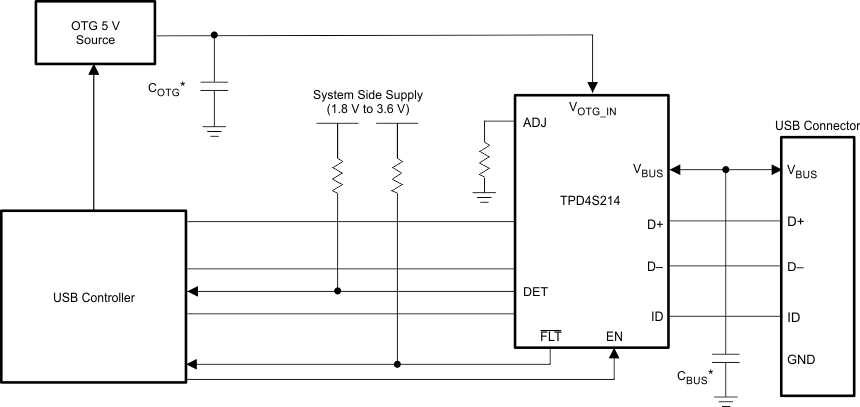
The TPD4S214 is a single-chip protection solution for USB On-the-Go (OTG) and other current limited USB applications. This device includes an integrated low RDS(ON) N-channel current limited switch for the OTG current supply to peripheral devices. TPD4S214 offers low capacitance transient voltage suppression (TVS) electrostatic discharge (ESD) clamping diodes for the D+, D–, and ID pins for both USB2.0 and USB3.0 applications. The VBUS pin can handle continuous voltage ranging from –7 V to 30 V. The over voltage lock-out (OVLO) at the VBUS pin ensures that if there is a fault condition at the VBUS line, TPD4S214 is able to isolate it and protect the internal circuitry from damage. Similarly, the under voltage lock out (UVLO) at the VOTG_IN pin ensures that there is no power drain from the internal OTG supply to external VBUS if VOTG_IN droops below a safe operating level. When EN is high, the OTG switch is activated and the FLT pin indicates whether there is a fault condition. The soft start feature waits 16 ms to turn on the OTG switch after all operating conditions are met.
Device Information(1)
| PART NUMBER | PACKAGE | BODY SIZE (MAX) |
|---|---|---|
| TPD4S214 | WCSP (12) | 1.39 mm × 1.69 mm |
- For all available packages, see the orderable addendum at the end of the datasheet.
4 Simplified Schematic