SLVSEL8 June 2018 TPD6S300A
PRODUCTION DATA.
- 1 Features
- 2 Applications
- 3 Description
- 4 Revision History
- 5 Device Comparison Table
- 6 Pin Configuration and Functions
- 7 Specifications
-
8 Detailed Description
- 8.1 Overview
- 8.2 Functional Block Diagram
- 8.3
Feature Description
- 8.3.1 4-Channels of Short-to-VBUS Overvoltage Protection (CC1, CC2, SBU1, SBU2 Pins or CC1, CC2, DP, DM Pins): 24-VDC Tolerant
- 8.3.2 6-Channels of IEC 61000-4-2 ESD Protection (CC1, CC2, SBU1, SBU2, DP, DM Pins)
- 8.3.3 CC1, CC2 Overvoltage Protection FETs 600 mA Capable for Passing VCONN Power
- 8.3.4 CC Dead Battery Resistors Integrated for Handling the Dead Battery Use Case in Mobile Devices
- 8.3.5 Advantages over TPD6S300
- 8.3.6 3-mm × 3-mm WQFN Package
- 8.4 Device Functional Modes
- 9 Application and Implementation
- 10Power Supply Recommendations
- 11Layout
- 12Device and Documentation Support
- 13Mechanical, Packaging, and Orderable Information
Package Options
Mechanical Data (Package|Pins)
- RUK|20
Thermal pad, mechanical data (Package|Pins)
- RUK|20
Orderable Information
3 Description
The TPD6S300A is a single-chip USB Type-C port protection device that provides 20-V Short-to-VBUS overvoltage and IEC ESD protection.
Since the release of the USB Type-C connector, many products and accessories for USB Type-C have been released that do not meet the USB Type-C specification. One example of this is USB Type-C Power Delivery adaptors that only place 20 V on the VBUS line. Another concern for USB Type-C is that mechanical twisting and sliding of the connector could short pins due to the close proximity they have in this small connector. This can cause 20-V VBUS to be shorted to the CC and SBU pins. Also due to the proximity of the pins in the Type-C connector, there is a heightened concern that debris and moisture will cause the 20-V VBUS pin to be shorted to the CC and SBU pins.
These non-ideal equipments and mechanical events make it necessary for the CC and SBU pins to be 20-V tolerant, even though the pins only operate at 5 V or lower. The TPD6S300A enables the CC and SBU pins to be 20-V tolerant without interfering with normal operation by providing overvoltage protection on the CC and SBU pins. The device places high voltage FETs in series on the SBU and CC lines. When a voltage above the OVP threshold is detected on these lines, the high voltage switches are opened up, isolating the rest of the system from the high voltage condition present on the connector.
Finally, most systems require IEC 61000-4-2 system level ESD protection for external pins. The TPD6S300A integrates IEC 61000-4-2 ESD protection for the CC1, CC2, SBU1, SBU2, DP, and DM pins, eliminating the need to place high voltage TVS diodes externally on the connector.
Device Information(1)
| PART NUMBER | PACKAGE | BODY SIZE (NOM) |
|---|---|---|
| TPD6S300A | WQFN (20) | 3.00 mm × 3.00 mm |
- For all available packages, see the orderable addendum at the end of the data sheet.
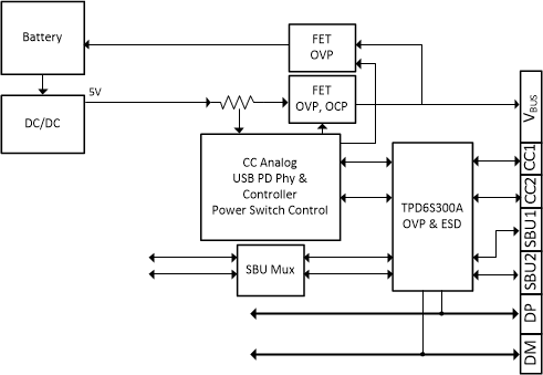
CC and SBU Over-Voltage Protection

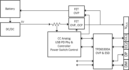
CC and DP/DM Over-Voltage Protection
