SLVSEL8 June   2018 TPD6S300A

PRODUCTION DATA.  

  1. Features
  2. Applications
  3. Description
    1.     CC and SBU Over-Voltage Protection
    2.     CC and DP/DM Over-Voltage Protection
  4. Revision History
  5. Device Comparison Table
  6. Pin Configuration and Functions
    1.     Pin Functions
  7. Specifications
    1. 7.1 Absolute Maximum Ratings
    2. 7.2 ESD Ratings—JEDEC Specification
    3. 7.3 ESD Ratings—IEC Specification
    4. 7.4 Recommended Operating Conditions
    5. 7.5 Thermal Information
    6. 7.6 Electrical Characteristics
    7. 7.7 Timing Requirements
    8. 7.8 Typical Characteristics
  8. Detailed Description
    1. 8.1 Overview
    2. 8.2 Functional Block Diagram
    3. 8.3 Feature Description
      1. 8.3.1 4-Channels of Short-to-VBUS Overvoltage Protection (CC1, CC2, SBU1, SBU2 Pins or CC1, CC2, DP, DM Pins): 24-VDC Tolerant
      2. 8.3.2 6-Channels of IEC 61000-4-2 ESD Protection (CC1, CC2, SBU1, SBU2, DP, DM Pins)
      3. 8.3.3 CC1, CC2 Overvoltage Protection FETs 600 mA Capable for Passing VCONN Power
      4. 8.3.4 CC Dead Battery Resistors Integrated for Handling the Dead Battery Use Case in Mobile Devices
      5. 8.3.5 Advantages over TPD6S300
        1. 8.3.5.1 Improved Dead Battery Performance
        2. 8.3.5.2 USB Type-C Port Stays Connected during an IEC 61000-4-2 ESD Strike
      6. 8.3.6 3-mm × 3-mm WQFN Package
    4. 8.4 Device Functional Modes
  9. Application and Implementation
    1. 9.1 Application Information
    2. 9.2 Typical Application
      1. 9.2.1 Design Requirements
      2. 9.2.2 Detailed Design Procedure
        1. 9.2.2.1 VBIAS Capacitor Selection
        2. 9.2.2.2 Dead Battery Operation
        3. 9.2.2.3 CC Line Capacitance
        4. 9.2.2.4 Additional ESD Protection on CC and SBU Lines
        5. 9.2.2.5 FLT Pin Operation
        6. 9.2.2.6 How to Connect Unused Pins
      3. 9.2.3 Application Curves
  10. 10Power Supply Recommendations
  11. 11Layout
    1. 11.1 Layout Guidelines
    2. 11.2 Layout Example
  12. 12Device and Documentation Support
    1. 12.1 Documentation Support
      1. 12.1.1 Related Documentation
    2. 12.2 Receiving Notification of Documentation Updates
    3. 12.3 Community Resources
    4. 12.4 Trademarks
    5. 12.5 Electrostatic Discharge Caution
    6. 12.6 Glossary
  13. 13Mechanical, Packaging, and Orderable Information

Package Options

Mechanical Data (Package|Pins)
Thermal pad, mechanical data (Package|Pins)
Orderable Information

Typical Characteristics
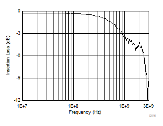
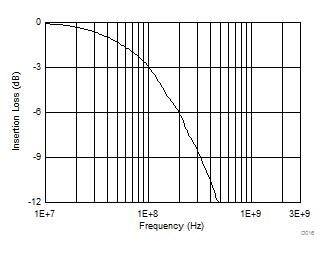
TPD6S300A D003_TPD8S300_Typ_Char.gif
Figure 1. SBU S21 BW
TPD6S300A D005_TPD8S300_Typ_Char.gif
Figure 3. SBU Short-to-VBUS 20 V
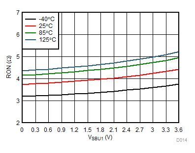
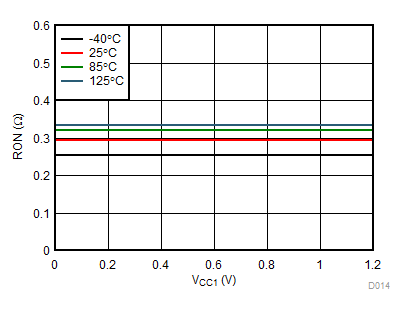
TPD6S300A D008_SLVSDD6.gif
Figure 5. SBU RON Flatness
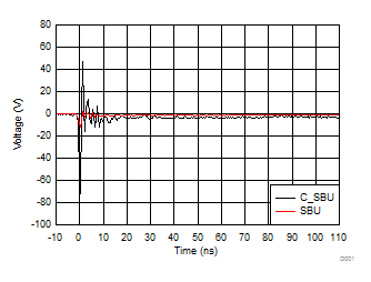
TPD6S300A D010_TPD8S300_Typ_Char.gif
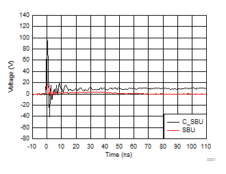
Figure 7. SBU IEC 61000-4-2 –4-kV Response Waveform
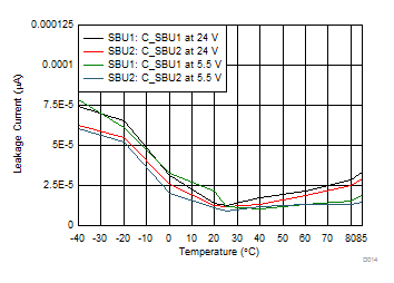
TPD6S300A D012_TPD8S300_Typ_Char.gif
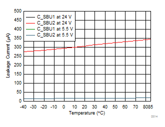
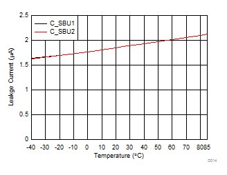
Figure 9. C_SBU OVP Leakage Current vs Ambient Temperature at 5.5 V and 24 V
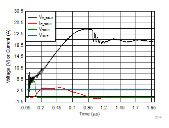
TPD6S300A D014_TPD8S300_Typ_Char.gif
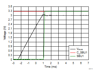
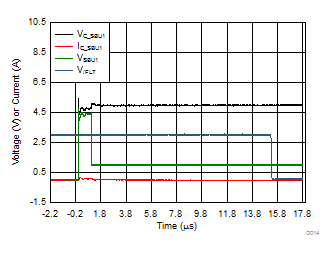
Figure 11. SBU FET Turnon Timing
TPD6S300A D016_TPD8S300_Typ_Char.gif
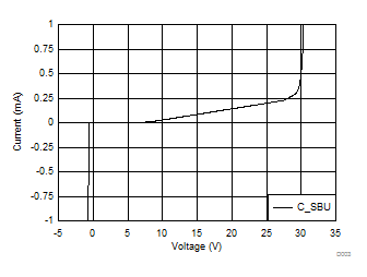
Figure 13. SBU IV Curve
TPD6S300A D017_TPD8S300_Typ_Char.gif
Figure 15. CC Short-to-VBUS 20 V
TPD6S300A D019_TPD8S300_Typ_Char.gif
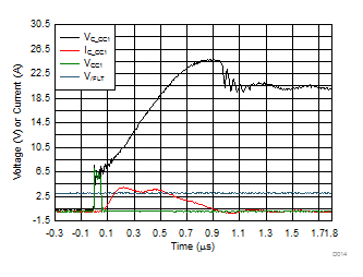
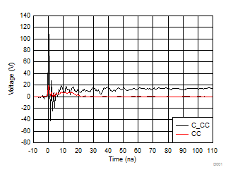
Figure 17. CC IEC 61000-4-2 8-kV Response Waveform
TPD6S300A D021_TPD8S300_Typ_Char.gif
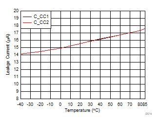
Figure 19. C_CC Path Leakage Current vs Ambient Temperature at C_CC = 5.5 V
TPD6S300A D023_TPD8S300_Typ_Char.gif
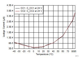
Figure 21. CC OVP Leakage Current vs Ambient Temperature at C_CC = 24 V
TPD6S300A D025_TPD8S300_Typ_Char.gif
Figure 23. C_CC TLP Curve Unpowered
TPD6S300A D027_TPD8S300_Typ_Char.gif
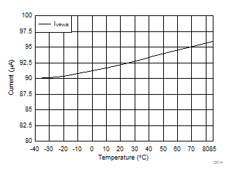
Figure 25. VPWR Supply Leakage vs Ambient Temperature at 3.6 V
TPD6S300A D029_TPD8S300_Typ_Char.gif
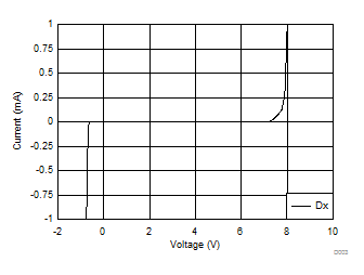
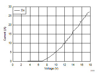
Figure 27. Dx IV Curve
TPD6S300A D004_TPD8S300_Typ_Char.gif
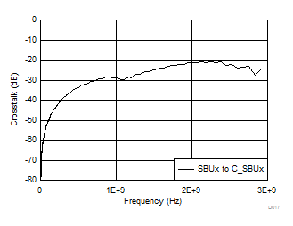
Figure 2. SBU Crosstalk
TPD6S300A D006_TPD8S300_Typ_Char.gif
Figure 4. SBU Short-to-VBUS 5 V
TPD6S300A D009_TPD8S300_Typ_Char.gif
Figure 6. SBU IEC 61000-4-2 4-kV Response Waveform
TPD6S300A D011_TPD8S300_Typ_Char.gif
Figure 8. SBU Path Leakage Current vs Ambient Temperature at 3.6 V
TPD6S300A D013_TPD8S300_Typ_Char.gif
Figure 10. SBU OVP Leakage Current vs Ambient Temperature at 5.5 V and 24 V
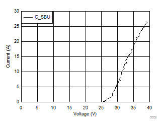
TPD6S300A D015_TPD8S300_Typ_Char.gif
Figure 12. C_SBU TLP Curve Unpowered
TPD6S300A D001_TPD8S300_Typ_Char.gif
Figure 14. CC S21 BW
TPD6S300A D018_SLVSDD6.gif
Figure 16. CC RON Flatness
TPD6S300A D020_TPD8S300_Typ_Char.gif
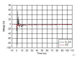
Figure 18. CC IEC 61000-4-2 –8-kV Response Waveform
TPD6S300A D022_TPD8S300_Typ_Char.gif
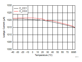
Figure 20. C_CC OVP Leakage Current vs Ambient Temperature at C_CC = 24 V
TPD6S300A D024_TPD8S300_Typ_Char.gif
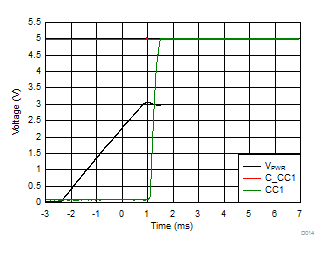
Figure 22. CC FET Turnon Timing
TPD6S300A D026_TPD8S300_Typ_Char.gif
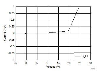
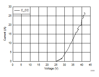
Figure 24. C_CC IV Curve
TPD6S300A D028_TPD8S300_Typ_Char.gif
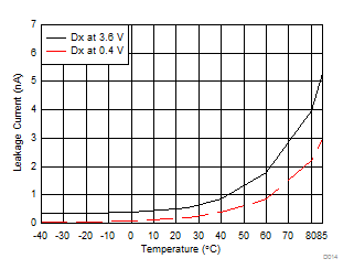
Figure 26. Dx Leakage Current vs Ambient Temperature at 0.4 V and 3.6 V
TPD6S300A D030_TPD8S300_Typ_Char.gif
Figure 28. Dx TLP Curve