SLIS149 June 2014 TPL0102-EP
PRODUCTION DATA.
- 1 Features
- 2 Applications
- 3 Description
- 4 Functional Block Diagram
- 5 Revision History
- 6 Pin Configuration and Functions
- 7 Specifications
-
8 Detailed Description
- 8.1 Overview
- 8.2 Functional Block Diagram
- 8.3 Feature Description
- 8.4 Device Functional Modes
- 8.5
Register Maps
- 8.5.1 Slave Address
- 8.5.2 TPL0102-EP Register Maps
- 8.5.3 IVRA (Initial Value Register for Potentiometer A)
- 8.5.4 WRA (Wiper Resistance Register for Potentiometer A)
- 8.5.5 IVRB (Initial Value Register for Potentiometer B)
- 8.5.6 WRB (Wiper Resistance Register for Potentiometer B)
- 8.5.7 ACR (Access Control Register)
- 9 Application and Implementation
- 10Layout
- 11Device and Documentation Support
- 12Mechanical, Packaging, and Orderable Information
Package Options
Mechanical Data (Package|Pins)
- PW|14
Thermal pad, mechanical data (Package|Pins)
- PW|14
Orderable Information
9 Application and Implementation
9.1 Application Information
In a simple operational amplifier configuration, like the one found in Figure 21, the TPL0102-EP is used to control the gain and offset voltage of the operational amplifier. Using the TPL0102-EP in a rheostat mode (like Rheostat Mode A in Figure 19), the gain setting of the negative feedback loop can be adjusted freely. To have maximum control of the offset voltage correction of the operational amplifier, the voltage divider mode can be used; giving the user an increased amount of control and precision for systems sensitive to DC offset.
9.2 Typical Application
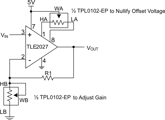 Figure 21. Offset Voltage and Gain Adjustment