SLIS149 June 2014 TPL0102-EP
PRODUCTION DATA.
- 1 Features
- 2 Applications
- 3 Description
- 4 Functional Block Diagram
- 5 Revision History
- 6 Pin Configuration and Functions
- 7 Specifications
-
8 Detailed Description
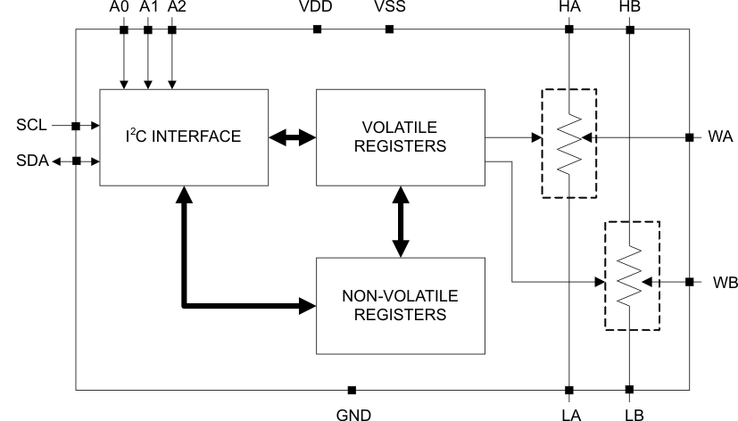
- 8.1 Overview
- 8.2 Functional Block Diagram
- 8.3 Feature Description
- 8.4 Device Functional Modes
- 8.5
Register Maps
- 8.5.1 Slave Address
- 8.5.2 TPL0102-EP Register Maps
- 8.5.3 IVRA (Initial Value Register for Potentiometer A)
- 8.5.4 WRA (Wiper Resistance Register for Potentiometer A)
- 8.5.5 IVRB (Initial Value Register for Potentiometer B)
- 8.5.6 WRB (Wiper Resistance Register for Potentiometer B)
- 8.5.7 ACR (Access Control Register)
- 9 Application and Implementation
- 10Layout
- 11Device and Documentation Support
- 12Mechanical, Packaging, and Orderable Information
Package Options
Mechanical Data (Package|Pins)
- PW|14
Thermal pad, mechanical data (Package|Pins)
- PW|14
Orderable Information
8 Detailed Description
8.1 Overview
The TPL0102-EP is a two-channel, linear-taper digital potentiometer with 256 wiper positions. Each potentiometer can be used as a three-pin potentiometer or as a two-pin rheostat. The TPL0102-EP-100 has an end-to-end resistance of 100 kΩ.
The TPL0102-EP has non-volatile memory (EEPROM) which can be used to store the wiper position. When the device is powered down, the last value stored in the IVR register will be maintained in the non-volatile memory. When power is restored, the contents of the IVR register are recalled and loaded into the corresponding WR register to set the wipers to the initial position. The internal registers of the TPL0102-EP can be accessed using the I2C interface.
The position of the wiper pin is controlled by the value in the WR 8-bit register. When the WR contains all zeroes, the wiper pin W is closest to its L (low) pin. As the value of the WR increases from all zeroes to all ones (255 decimal), the wiper moves monotonically from the position closest to L to the position closest to H. At the same time, the resistance between W and L increases monotonically, whereas the resistance between W and H decreases monotonically.
8.2 Functional Block Diagram
8.3 Feature Description
Table 1. Summary of Features
| Feature | TPL0102-EP |
|---|---|
| Number of potentiometers | 2 |
| Digital interface | I2C |
| Steps | 256 |
| Wiper memory | Non-volatile |
| Taper | Linear |
| End-to-end resistance | 100 kΩ |
| End-to-end resistance tolerance | 20% |
| Wiper resistance | 25 Ω (typ) |
8.3.1 Potentiometer Pin Description
8.3.1.1 HA, HB, LA, LB
The high (HA, HB) and low (LA, LB) pins of the TPL0102-EP are equivalent to the fixed pins of a mechanical potentiometer. The H and L pins do not have any polarity restrictions, i.e. H can be at a higher voltage than L, or L can be at a higher voltage than H. The WA and WB pins are the wipers and equivalent to the movable pin of a mechanical potentiometer. The position of the wiper is set using the WR register. With the WR register set to 255 decimal, the wiper is closest to the H pin, and with the WR register set to 0, the wiper is closest to the L pin.
8.3.1.2 SDA, SCL
SDA is a bi-directional serial data input/output pin for I2C communication. SDA is an open drain output and requires an external pull-up resistor.
SCL is the serial clock input for I2C communication. SCL requires an external pull-up resistor.
8.3.1.3 A0, A1, A2
These inputs are used to set the last three bits of the I2C address of the device. By using different values for A0, A1, A2, up to eight TPL0102-EP devices can be used on the same I2C bus.
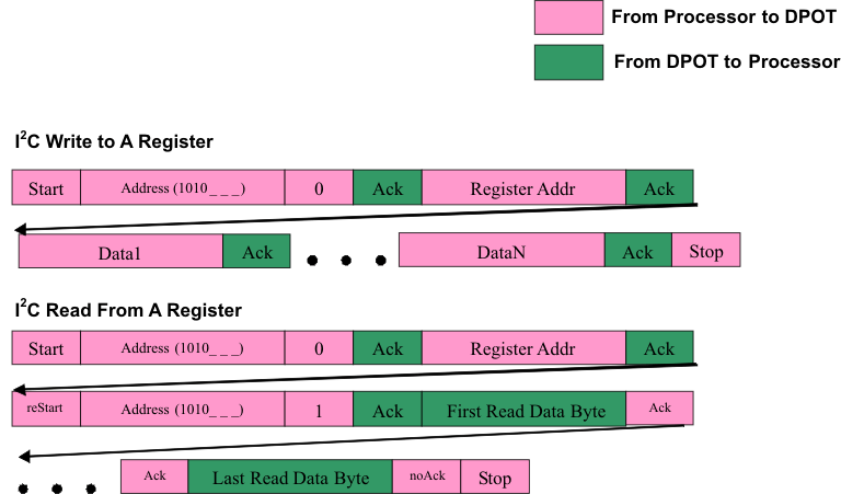 Figure 13. I2C Interface
The following is a sample sequence to set wipers of both potentiometers at mid-scale. Assume A0, A1, and A2 are 0 and device has just been powered up.
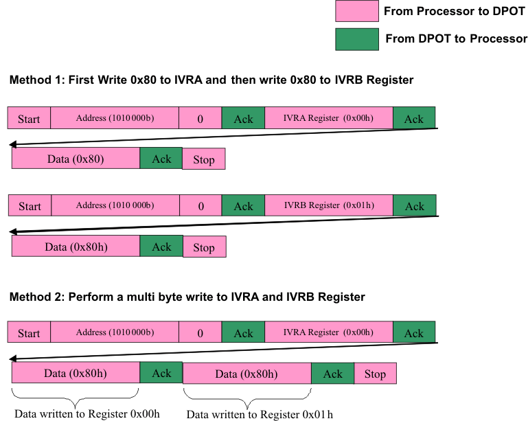 Figure 14. tI2C Interface Example
8.3.2 Standard I2C Interface Details
The bidirectional I2C bus consists of the serial clock (SCL) and serial data (SDA) lines. Both lines must be connected to a positive supply via a pullup resistor when connected to the output stages of a device. Data transfer may be initiated only when the bus is not busy.
I2C communication with this device is initiated by the master sending a start condition, a high-to-low transition on the SDA input/output while the SCL input is high (see Figure 15). After the start condition, the device address byte is sent, MSB first, including the data direction bit (R/W). This device does not respond to the general call address. After receiving the valid address byte, this device responds with an ACK, a low on the SDA input/output during the high of the ACK-related clock pulse
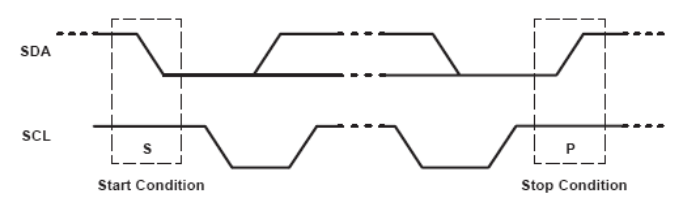 Figure 15. Definition of Start and Stop Conditions
The data byte follows the address ACK. The R/W bit is kept low for transfer from the master to the slave. The data byte is followed by an ACK sent from this device. Data are output only if complete bytes are received and acknowledged. The output data is valid at time (tpv) after the low-to-high transition of SCL, during the clock cycle for the ACK. On the I2C bus, only one data bit is transferred during each clock pulse. The data on the SDA line must remain stable during the high pulse of the clock period, as changes in the data line at this time are interpreted as control commands (start or stop) (see Figure 16).
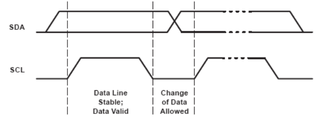 Figure 16. Bit Transfer
A stop condition, a low-to-high transition on the SDA input/output while the SCL input is high, is sent by the master (see Figure 15).
The number of data bytes transferred between the start and the stop conditions from transmitter to receiver is not limited. Each byte of eight bits is followed by one ACK bit. The transmitter must release the SDA line before the receiver can send an ACK bit.
A slave receiver that is addressed must generate an ACK after the reception of each byte. The device that acknowledges has to pull down the SDA line during the ACK clock pulse so that the SDA line is stable low during the high pulse of the ACK-related clock period (see Figure 17). Setup and hold times must be taken into account.
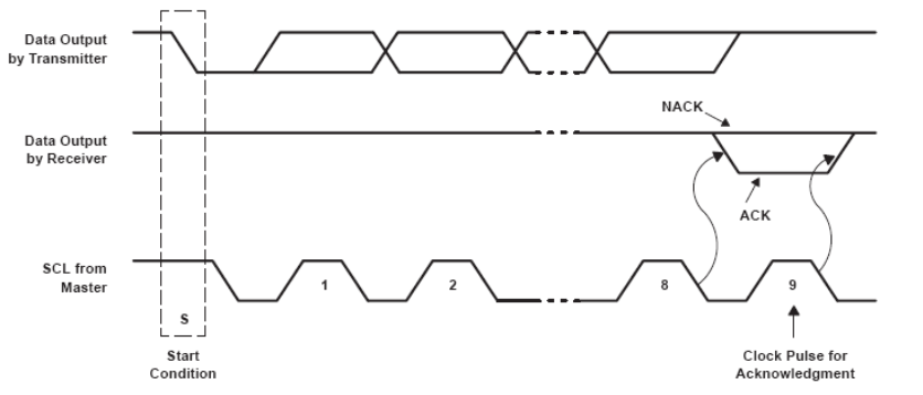 Figure 17. Acknowledgment on the I2C Bus
8.3.3 Ideal Resistance Values
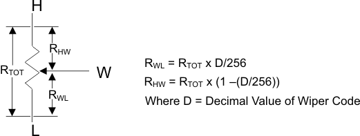 Figure 18.
Table 2 shows the ideal values for DPOT with end-to-end resistance of 100 kΩ. The absolute values of resistance can vary significantly, but the ratio (RWL / RHW) is extremely accurate.
Table 2.
| Step | Binary | RWL (kΩ) | RHW (kΩ) | RWL / RHW |
|---|---|---|---|---|
| 0 | 0 | 0.00 | 100.00 | 0.00 |
| 1 | 1 | 0.39 | 99.61 | 0.00 |
| 2 | 10 | 0.78 | 99.22 | 0.01 |
| 3 | 11 | 1.17 | 98.83 | 0.01 |
| 4 | 100 | 1.56 | 98.44 | 0.02 |
| 5 | 101 | 1.95 | 98.05 | 0.02 |
| 6 | 110 | 2.34 | 97.66 | 0.02 |
| 7 | 111 | 2.73 | 97.27 | 0.03 |
| 8 | 1000 | 3.13 | 96.88 | 0.03 |
| 9 | 1001 | 3.52 | 96.48 | 0.04 |
| 10 | 1010 | 3.91 | 96.09 | 0.04 |
| 11 | 1011 | 4.30 | 95.70 | 0.04 |
| 12 | 1100 | 4.69 | 95.31 | 0.05 |
| 13 | 1101 | 5.08 | 94.92 | 0.05 |
| 14 | 1110 | 5.47 | 94.53 | 0.06 |
| 15 | 1111 | 5.86 | 94.14 | 0.06 |
| 16 | 10000 | 6.25 | 93.75 | 0.07 |
| 17 | 10001 | 6.64 | 93.36 | 0.07 |
| 18 | 10010 | 7.03 | 92.97 | 0.08 |
| 19 | 10011 | 7.42 | 92.58 | 0.08 |
| 20 | 10100 | 7.81 | 92.19 | 0.08 |
| 21 | 10101 | 8.20 | 91.80 | 0.09 |
| 22 | 10110 | 8.59 | 91.41 | 0.09 |
| 23 | 10111 | 8.98 | 91.02 | 0.10 |
| 24 | 11000 | 9.38 | 90.63 | 0.10 |
| 25 | 11001 | 9.77 | 90.23 | 0.11 |
| 26 | 11010 | 10.16 | 89.84 | 0.11 |
| 27 | 11011 | 10.55 | 89.45 | 0.12 |
| 28 | 11100 | 10.94 | 89.06 | 0.12 |
| 29 | 11101 | 11.33 | 88.67 | 0.13 |
| 30 | 11110 | 11.72 | 88.28 | 0.13 |
| 31 | 11111 | 12.11 | 87.89 | 0.14 |
| 32 | 100000 | 12.50 | 87.50 | 0.14 |
| 33 | 100001 | 12.89 | 87.11 | 0.15 |
| 34 | 100010 | 13.28 | 86.72 | 0.15 |
| 35 | 100011 | 13.67 | 86.33 | 0.16 |
| 36 | 100100 | 14.06 | 85.94 | 0.16 |
| 37 | 100101 | 14.45 | 85.55 | 0.17 |
| 38 | 100110 | 14.84 | 85.16 | 0.17 |
| 39 | 100111 | 15.23 | 84.77 | 0.18 |
| 40 | 101000 | 15.63 | 84.38 | 0.19 |
| 41 | 101001 | 16.02 | 83.98 | 0.19 |
| 42 | 101010 | 16.41 | 83.59 | 0.20 |
| 43 | 101011 | 16.80 | 83.20 | 0.20 |
| 44 | 101100 | 17.19 | 82.81 | 0.21 |
| 45 | 101101 | 17.58 | 82.42 | 0.21 |
| 46 | 101110 | 17.97 | 82.03 | 0.22 |
| 47 | 101111 | 18.36 | 81.64 | 0.22 |
| 48 | 110000 | 18.75 | 81.25 | 0.23 |
| 49 | 110001 | 19.14 | 80.86 | 0.24 |
| 50 | 110010 | 19.53 | 80.47 | 0.24 |
| 51 | 110011 | 19.92 | 80.08 | 0.25 |
| 52 | 110100 | 20.31 | 79.69 | 0.25 |
| 53 | 110101 | 20.70 | 79.30 | 0.26 |
| 54 | 110110 | 21.09 | 78.91 | 0.27 |
| 55 | 110111 | 21.48 | 78.52 | 0.27 |
| 56 | 111000 | 21.88 | 78.13 | 0.28 |
| 57 | 111001 | 22.27 | 77.73 | 0.29 |
| 58 | 111010 | 22.66 | 77.34 | 0.29 |
| 59 | 111011 | 23.05 | 76.95 | 0.30 |
| 60 | 111100 | 23.44 | 76.56 | 0.31 |
| 61 | 111101 | 23.83 | 76.17 | 0.31 |
| 62 | 111110 | 24.22 | 75.78 | 0.32 |
| 63 | 111111 | 24.61 | 75.39 | 0.33 |
| 64 | 1000000 | 25.00 | 75.00 | 0.33 |
| 65 | 1000001 | 25.39 | 74.61 | 0.34 |
| 66 | 1000010 | 25.78 | 74.22 | 0.35 |
| 67 | 1000011 | 26.17 | 73.83 | 0.35 |
| 68 | 1000100 | 26.56 | 73.44 | 0.36 |
| 69 | 1000101 | 26.95 | 73.05 | 0.37 |
| 70 | 1000110 | 27.34 | 72.66 | 0.38 |
| 71 | 1000111 | 27.73 | 72.27 | 0.38 |
| 72 | 1001000 | 28.13 | 71.88 | 0.39 |
| 73 | 1001001 | 28.52 | 71.48 | 0.40 |
| 74 | 1001010 | 28.91 | 71.09 | 0.41 |
| 75 | 1001011 | 29.30 | 70.70 | 0.41 |
| 76 | 1001100 | 29.69 | 70.31 | 0.42 |
| 77 | 1001101 | 30.08 | 69.92 | 0.43 |
| 78 | 1001110 | 30.47 | 69.53 | 0.44 |
| 79 | 1001111 | 30.86 | 69.14 | 0.45 |
| 80 | 1010000 | 31.25 | 68.75 | 0.45 |
| 81 | 1010001 | 31.64 | 68.36 | 0.46 |
| 82 | 1010010 | 32.03 | 67.97 | 0.47 |
| 83 | 1010011 | 32.42 | 67.58 | 0.48 |
| 84 | 1010100 | 32.81 | 67.19 | 0.49 |
| 85 | 1010101 | 33.20 | 66.80 | 0.50 |
| 86 | 1010110 | 33.59 | 66.41 | 0.51 |
| 87 | 1010111 | 33.98 | 66.02 | 0.51 |
| 88 | 1011000 | 34.38 | 65.63 | 0.52 |
| 89 | 1011001 | 34.77 | 65.23 | 0.53 |
| 90 | 1011010 | 35.16 | 64.84 | 0.54 |
| 91 | 1011011 | 35.55 | 64.45 | 0.55 |
| 92 | 1011100 | 35.94 | 64.06 | 0.56 |
| 93 | 1011101 | 36.33 | 63.67 | 0.57 |
| 94 | 1011110 | 36.72 | 63.28 | 0.58 |
| 95 | 1011111 | 37.11 | 62.89 | 0.59 |
| 96 | 1100000 | 37.50 | 62.50 | 0.60 |
| 97 | 1100001 | 37.89 | 62.11 | 0.61 |
| 98 | 1100010 | 38.28 | 61.72 | 0.62 |
| 99 | 1100011 | 38.67 | 61.33 | 0.63 |
| 100 | 1100100 | 39.06 | 60.94 | 0.64 |
| 101 | 1100101 | 39.45 | 60.55 | 0.65 |
| 102 | 1100110 | 39.84 | 60.16 | 0.66 |
| 103 | 1100111 | 40.23 | 59.77 | 0.67 |
| 104 | 1101000 | 40.63 | 59.38 | 0.68 |
| 105 | 1101001 | 41.02 | 58.98 | 0.70 |
| 106 | 1101010 | 41.41 | 58.59 | 0.71 |
| 107 | 1101011 | 41.80 | 58.20 | 0.72 |
| 108 | 1101100 | 42.19 | 57.81 | 0.73 |
| 109 | 1101101 | 42.58 | 57.42 | 0.74 |
| 110 | 1101110 | 42.97 | 57.03 | 0.75 |
| 111 | 1101111 | 43.36 | 56.64 | 0.77 |
| 112 | 1110000 | 43.75 | 56.25 | 0.78 |
| 113 | 1110001 | 44.14 | 55.86 | 0.79 |
| 114 | 1110010 | 44.53 | 55.47 | 0.80 |
| 115 | 1110011 | 44.92 | 55.08 | 0.82 |
| 116 | 1110100 | 45.31 | 54.69 | 0.83 |
| 117 | 1110101 | 45.70 | 54.30 | 0.84 |
| 118 | 1110110 | 46.09 | 53.91 | 0.86 |
| 119 | 1110111 | 46.48 | 53.52 | 0.87 |
| 120 | 1111000 | 46.88 | 53.13 | 0.88 |
| 121 | 1111001 | 47.27 | 52.73 | 0.90 |
| 122 | 1111010 | 47.66 | 52.34 | 0.91 |
| 123 | 1111011 | 48.05 | 51.95 | 0.92 |
| 124 | 1111100 | 48.44 | 51.56 | 0.94 |
| 125 | 1111101 | 48.83 | 51.17 | 0.95 |
| 126 | 1111110 | 49.22 | 50.78 | 0.97 |
| 127 | 1111111 | 49.61 | 50.39 | 0.98 |
| 128 | 10000000 | 50.00 | 50.00 | 1.00 |
| 129 | 10000001 | 50.39 | 49.61 | 1.02 |
| 130 | 10000010 | 50.78 | 49.22 | 1.03 |
| 131 | 10000011 | 51.17 | 48.83 | 1.05 |
| 132 | 10000100 | 51.56 | 48.44 | 1.06 |
| 133 | 10000101 | 51.95 | 48.05 | 1.08 |
| 134 | 10000110 | 52.34 | 47.66 | 1.10 |
| 135 | 10000111 | 52.73 | 47.27 | 1.12 |
| 136 | 10001000 | 53.13 | 46.88 | 1.13 |
| 137 | 10001001 | 53.52 | 46.48 | 1.15 |
| 138 | 10001010 | 53.91 | 46.09 | 1.17 |
| 139 | 10001011 | 54.30 | 45.70 | 1.19 |
| 140 | 10001100 | 54.69 | 45.31 | 1.21 |
| 141 | 10001101 | 55.08 | 44.92 | 1.23 |
| 142 | 10001110 | 55.47 | 44.53 | 1.25 |
| 143 | 10001111 | 55.86 | 44.14 | 1.27 |
| 144 | 10010000 | 56.25 | 43.75 | 1.29 |
| 145 | 10010001 | 56.64 | 43.36 | 1.31 |
| 146 | 10010010 | 57.03 | 42.97 | 1.33 |
| 147 | 10010011 | 57.42 | 42.58 | 1.35 |
| 148 | 10010100 | 57.81 | 42.19 | 1.37 |
| 149 | 10010101 | 58.20 | 41.80 | 1.39 |
| 150 | 10010110 | 58.59 | 41.41 | 1.42 |
| 151 | 10010111 | 58.98 | 41.02 | 1.44 |
| 152 | 10011000 | 59.38 | 40.63 | 1.46 |
| 153 | 10011001 | 59.77 | 40.23 | 1.49 |
| 154 | 10011010 | 60.16 | 39.84 | 1.51 |
| 155 | 10011011 | 60.55 | 39.45 | 1.53 |
| 156 | 10011100 | 60.94 | 39.06 | 1.56 |
| 157 | 10011101 | 61.33 | 38.67 | 1.59 |
| 158 | 10011110 | 61.72 | 38.28 | 1.61 |
| 159 | 10011111 | 62.11 | 37.89 | 1.64 |
| 160 | 10100000 | 62.50 | 37.50 | 1.67 |
| 161 | 10100001 | 62.89 | 37.11 | 1.69 |
| 162 | 10100010 | 63.28 | 36.72 | 1.72 |
| 163 | 10100011 | 63.67 | 36.33 | 1.75 |
| 164 | 10100100 | 64.06 | 35.94 | 1.78 |
| 165 | 10100101 | 64.45 | 35.55 | 1.81 |
| 166 | 10100110 | 64.84 | 35.16 | 1.84 |
| 167 | 10100111 | 65.23 | 34.77 | 1.88 |
| 168 | 10101000 | 65.63 | 34.38 | 1.91 |
| 169 | 10101001 | 66.02 | 33.98 | 1.94 |
| 170 | 10101010 | 66.41 | 33.59 | 1.98 |
| 171 | 10101011 | 66.80 | 33.20 | 2.01 |
| 172 | 10101100 | 67.19 | 32.81 | 2.05 |
| 173 | 10101101 | 67.58 | 32.42 | 2.08 |
| 174 | 10101110 | 67.97 | 32.03 | 2.12 |
| 175 | 10101111 | 68.36 | 31.64 | 2.16 |
| 176 | 10110000 | 68.75 | 31.25 | 2.20 |
| 177 | 10110001 | 69.14 | 30.86 | 2.24 |
| 178 | 10110010 | 69.53 | 30.47 | 2.28 |
| 179 | 10110011 | 69.92 | 30.08 | 2.32 |
| 180 | 10110100 | 70.31 | 29.69 | 2.37 |
| 181 | 10110101 | 70.70 | 29.30 | 2.41 |
| 182 | 10110110 | 71.09 | 28.91 | 2.46 |
| 183 | 10110111 | 71.48 | 28.52 | 2.51 |
| 184 | 10111000 | 71.88 | 28.13 | 2.56 |
| 185 | 10111001 | 72.27 | 27.73 | 2.61 |
| 186 | 10111010 | 72.66 | 27.34 | 2.66 |
| 187 | 10111011 | 73.05 | 26.95 | 2.71 |
| 188 | 10111100 | 73.44 | 26.56 | 2.76 |
| 189 | 10111101 | 73.83 | 26.17 | 2.82 |
| 190 | 10111110 | 74.22 | 25.78 | 2.88 |
| 191 | 10111111 | 74.61 | 25.39 | 2.94 |
| 192 | 11000000 | 75.00 | 25.00 | 3.00 |
| 193 | 11000001 | 75.39 | 24.61 | 3.06 |
| 194 | 11000010 | 75.78 | 24.22 | 3.13 |
| 195 | 11000011 | 76.17 | 23.83 | 3.20 |
| 196 | 11000100 | 76.56 | 23.44 | 3.27 |
| 197 | 11000101 | 76.95 | 23.05 | 3.34 |
| 198 | 11000110 | 77.34 | 22.66 | 3.41 |
| 199 | 11000111 | 77.73 | 22.27 | 3.49 |
| 200 | 11001000 | 78.13 | 21.88 | 3.57 |
| 201 | 11001001 | 78.52 | 21.48 | 3.65 |
| 202 | 11001010 | 78.91 | 21.09 | 3.74 |
| 203 | 11001011 | 79.30 | 20.70 | 3.83 |
| 204 | 11001100 | 79.69 | 20.31 | 3.92 |
| 205 | 11001101 | 80.08 | 19.92 | 4.02 |
| 206 | 11001110 | 80.47 | 19.53 | 4.12 |
| 207 | 11001111 | 80.86 | 19.14 | 4.22 |
| 208 | 11010000 | 81.25 | 18.75 | 4.33 |
| 209 | 11010001 | 81.64 | 18.36 | 4.45 |
| 210 | 11010010 | 82.03 | 17.97 | 4.57 |
| 211 | 11010011 | 82.42 | 17.58 | 4.69 |
| 212 | 11010100 | 82.81 | 17.19 | 4.82 |
| 213 | 11010101 | 83.20 | 16.80 | 4.95 |
| 214 | 11010110 | 83.59 | 16.41 | 5.10 |
| 215 | 11010111 | 83.98 | 16.02 | 5.24 |
| 216 | 11011000 | 84.38 | 15.63 | 5.40 |
| 217 | 11011001 | 84.77 | 15.23 | 5.56 |
| 218 | 11011010 | 85.16 | 14.84 | 5.74 |
| 219 | 11011011 | 85.55 | 14.45 | 5.92 |
| 220 | 11011100 | 85.94 | 14.06 | 6.11 |
| 221 | 11011101 | 86.33 | 13.67 | 6.31 |
| 222 | 11011110 | 86.72 | 13.28 | 6.53 |
| 223 | 11011111 | 87.11 | 12.89 | 6.76 |
| 224 | 11100000 | 87.50 | 12.50 | 7.00 |
| 225 | 11100001 | 87.89 | 12.11 | 7.26 |
| 226 | 11100010 | 88.28 | 11.72 | 7.53 |
| 227 | 11100011 | 88.67 | 11.33 | 7.83 |
| 228 | 11100100 | 89.06 | 10.94 | 8.14 |
| 229 | 11100101 | 89.45 | 10.55 | 8.48 |
| 230 | 11100110 | 89.84 | 10.16 | 8.85 |
| 231 | 11100111 | 90.23 | 9.77 | 9.24 |
| 232 | 11101000 | 90.63 | 9.38 | 9.67 |
| 233 | 11101001 | 91.02 | 8.98 | 10.13 |
| 234 | 11101010 | 91.41 | 8.59 | 10.64 |
| 235 | 11101011 | 91.80 | 8.20 | 11.19 |
| 236 | 11101100 | 92.19 | 7.81 | 11.80 |
| 237 | 11101101 | 92.58 | 7.42 | 12.47 |
| 238 | 11101110 | 92.97 | 7.03 | 13.22 |
| 239 | 11101111 | 93.36 | 6.64 | 14.06 |
| 240 | 11110000 | 93.75 | 6.25 | 15.00 |
| 241 | 11110001 | 94.14 | 5.86 | 16.07 |
| 242 | 11110010 | 94.53 | 5.47 | 17.29 |
| 243 | 11110011 | 94.92 | 5.08 | 18.69 |
| 244 | 11110100 | 95.31 | 4.69 | 20.33 |
| 245 | 11110101 | 95.70 | 4.30 | 22.27 |
| 246 | 11110110 | 96.09 | 3.91 | 24.60 |
| 247 | 11110111 | 96.48 | 3.52 | 27.44 |
| 248 | 11111000 | 96.88 | 3.13 | 31.00 |
| 249 | 11111001 | 97.27 | 2.73 | 35.57 |
| 250 | 11111010 | 97.66 | 2.34 | 41.67 |
| 251 | 11111011 | 98.05 | 1.95 | 50.20 |
| 252 | 11111100 | 98.44 | 1.56 | 63.00 |
| 253 | 11111101 | 98.83 | 1.17 | 84.33 |
| 254 | 11111110 | 99.22 | 0.78 | 127.00 |
| 255 | 11111111 | 99.61 | 0.3 | 255.00 |
8.4 Device Functional Modes
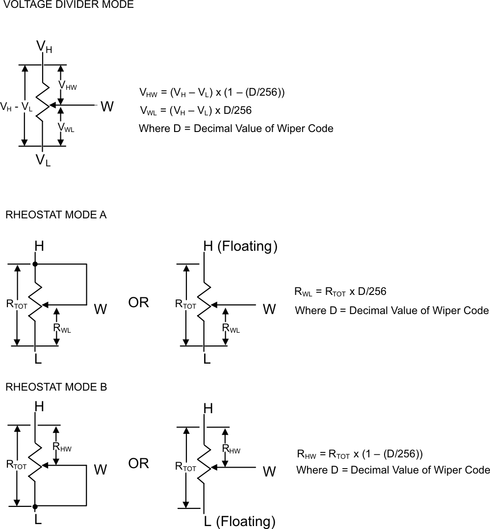 Figure 19. Digital Potentiometer Configurations
8.5 Register Maps
8.5.1 Slave Address
| Bit 7 (MSB) |
Bit 6 | Bit 5 | Bit 4 | Bit 3 | Bit 2 | Bit 2 | Bit 0 (LSB) |
|---|---|---|---|---|---|---|---|
| 1 | 0 | 1 | 0 | A2 | A1 | A0 | R/W |
8.5.2 TPL0102-EP Register Maps
| REGISTER ADDRESS (HEX) | NON-VOLATILE | VOLATILE |
|---|---|---|
| 0 | IVRA | WRA |
| 1 | IVRB | WRB |
| 2 | General purpose | N/A |
| 3 | General purpose | N/A |
| 4 | General purpose | N/A |
| 5 | General purpose | N/A |
| 6 | General purpose | N/A |
| 7 | General purpose | N/A |
| 8 | General purpose | N/A |
| 9 | General purpose | N/A |
| A | General purpose | N/A |
| B | General purpose | N/A |
| C | General purpose | N/A |
| E | General purpose | N/A |
| D | General purpose | N/A |
| F | Reserved | |
| 10 | N/A | ACR |
8.5.3 IVRA (Initial Value Register for Potentiometer A)
- Register address: 00H
- Factory programmed value: 80H
- Type: non-volatile write/read
| NAME | SIZE (BITS) | DESCRIPTION | ||
|---|---|---|---|---|
| IVRA | 8 | Non-volatile register to store wiper position for potentiometer A | ||
8.5.4 WRA (Wiper Resistance Register for Potentiometer A)
- Register address: 00H
- Reset value: same as IVRA
- Type: volatile write/read
| NAME | SIZE (BITS) | DESCRIPTION | ||
|---|---|---|---|---|
| WRA | 8 | Volatile register to change wiper position for potentiometer A | ||
8.5.5 IVRB (Initial Value Register for Potentiometer B)
- Register address: 01H
- Factory programmed value: 80H
- Type: non-volatile write/read
| NAME | SIZE (BITS) | DESCRIPTION | ||
|---|---|---|---|---|
| IVRB | 8 | Non-volatile register to store wiper position for potentiometer B | ||
8.5.6 WRB (Wiper Resistance Register for Potentiometer B)
- Register address: 01H
- Reset value: same as IVRB
- Type: volatile write/read
| NAME | SIZE (BITS) | DESCRIPTION | ||
|---|---|---|---|---|
| WRB | 8 | Volatile register to change wiper position for potentiometer B | ||
8.5.7 ACR (Access Control Register)
- Register address: 00H
- Reset value: 40H
- Type: non-volatile write/read
| NAME | SIZE (BITS) | DESCRIPTION | |||||||
|---|---|---|---|---|---|---|---|---|---|
| IVRA | 8 | Non-volatile register to store wiper position for potentiometer A | |||||||
| ACR | 8 | Bit 7 | Bit 6 | Bit 5 | Bit 4 | Bit 3 | Bit 2 | Bit 1 | Bit 0 |
| VOL | SHDN | WIP | 0 | 0 | 0 | 0 | 0 | ||
| Default Value | 0 | 1 | 0 | 0 | 0 | 0 | 0 | 0 | |
| NAME | SIZE (BITS) | DESCRIPTION | ||
|---|---|---|---|---|
| VOL | 1 | 0: Non-volatile registers (IVRA, IVRB) are accessible. Value written to IVRi register is also written to the corresponding WRi. | ||
| 1: Only volatile registers (WRi) are accessible. | ||||
| SHDN | 1 | 0: Shut-down mode is enabled. Potentiometers are in shut-down mode. (see Figure 20) |
||
| 1: Shut-down mode is disabled | ||||
| WIP (read-only bit) | 1 | 0: Non-volatile write operation is not in progress | ||
| 1: Non-volatile write operation is in progress (it is not possible to write to the WRi or ACR while WIP = 1) | ||||
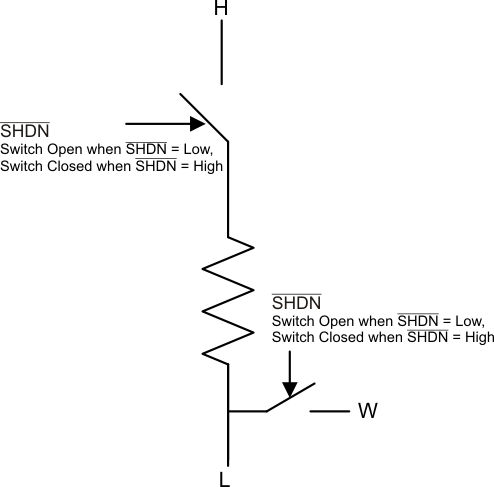 Figure 20. Potentiometer in Shut-Down Mode