SLIS144B September   2011  – February 2017

PRODUCTION DATA.  

  1. Features
  2. Applications
  3. Description
  4. Revision History
  5. Device Comparison Table
  6. Pin Configuration and Functions
  7. Specifications
    1. 7.1 Absolute Maximum Ratings
    2. 7.2 ESD Ratings
    3. 7.3 Recommended Operating Conditions
    4. 7.4 Thermal Information
    5. 7.5 Electrical Characteristics
    6. 7.6 Timing Requirements
    7. 7.7 Typical Characteristics
  8. Parameter Measurement Information
  9. Detailed Description
    1. 9.1 Overview
    2. 9.2 Functional Block Diagram
    3. 9.3 Feature Description
    4. 9.4 Device Functional Modes
      1. 9.4.1 Voltage Divider Mode
    5. 9.5 Programming
      1. 9.5.1 I2C General Operation and Overview
        1. 9.5.1.1 START and STOP Conditions
        2. 9.5.1.2 Data Validity and Byte Formation
        3. 9.5.1.3 Acknowledge (ACK) and Not Acknowledge (NACK)
        4. 9.5.1.4 Repeated Start
      2. 9.5.2 Programing with I2C
        1. 9.5.2.1 Write Operation
        2. 9.5.2.2 Read Operation
    6. 9.6 Register Maps
      1. 9.6.1 Slave Address
      2. 9.6.2 Register Address
  10. 10Application and Implementation
    1. 10.1 Application Information
    2. 10.2 Typical Application
      1. 10.2.1 Design Requirements
      2. 10.2.2 Detailed Design Procedure
      3. 10.2.3 Application Curve
  11. 11Power Supply Recommendations
    1. 11.1 Power Sequence
    2. 11.2 Power-On Reset Requirements
    3. 11.3 I2C Communication After Power Up
    4. 11.4 Wiper Position While Unpowered and After Power Up
  12. 12Layout
    1. 12.1 Layout Guidelines
    2. 12.2 Layout Example
  13. 13Device and Documentation Support
    1. 13.1 Documentation Support
      1. 13.1.1 Related Documentation
    2. 13.2 Related Links
    3. 13.3 Receiving Notification of Documentation Updates
    4. 13.4 Community Resources
    5. 13.5 Trademarks
    6. 13.6 Electrostatic Discharge Caution
    7. 13.7 Glossary
  14. 14Mechanical, Packaging, and Orderable Information

Package Options

Mechanical Data (Package|Pins)
Thermal pad, mechanical data (Package|Pins)
Orderable Information

Parameter Measurement Information

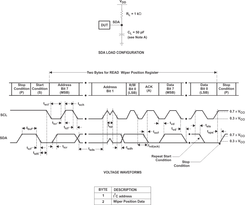
TPL0401A TPL0401B pmi_i2c_slis182.gif
CL includes probe and jig capacitance. tocf is measured with CL of 10 pF or 400 pF.
All inputs are supplied by generators having the following characteristics: PRR ≤ 10 MHz, ZO = 50 Ω, tr/tf ≤ 30 ns.
All parameters and waveforms are not applicable to all devices.
Figure 9. I2C Interface Load Circuit and Voltage Waveforms
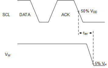
TPL0401A TPL0401B tsw_slis182.gif
Code change is from 0×40 to 0×00
All inputs are supplied by generators having the following characteristics: PRR ≤ 10 MHz, ZO = 50 Ω, tr/tf ≤ 30 ns.
Figure 10. Switch Time Waveform (tSW)