SLIS144B September 2011 – February 2017
PRODUCTION DATA.
- 1 Features
- 2 Applications
- 3 Description
- 4 Revision History
- 5 Device Comparison Table
- 6 Pin Configuration and Functions
- 7 Specifications
- 8 Parameter Measurement Information
- 9 Detailed Description
- 10Application and Implementation
- 11Power Supply Recommendations
- 12Layout
- 13Device and Documentation Support
- 14Mechanical, Packaging, and Orderable Information
Package Options
Mechanical Data (Package|Pins)
- DCK|6
Thermal pad, mechanical data (Package|Pins)
- DCK|6
Orderable Information
7 Specifications
7.1 Absolute Maximum Ratings
over operating free-air temperature range (unless otherwise noted) (1)| MIN | MAX | UNIT | |||
|---|---|---|---|---|---|
| VDD | Supply voltage | VDD to GND | –0.3 | 7 | V |
| IH, IL, IW | Continuous current | ±5 | mA | ||
| VI | Digital input pins (SDA, SCL) | –0.3 | VDD + 0.3 | V | |
| Potentiometer pins (H, W) | –0.3 | VDD + 0.3 | |||
| TJ(MAX) | Maximum junction temperature | 130 | °C | ||
| Tstg | Storage temperature | –65 | 150 | °C | |
(1) Stresses beyond those listed under Absolute Maximum Ratings may cause permanent damage to the device. These are stress ratings only, which do not imply functional operation of the device at these or any other conditions beyond those indicated under Recommended Operating Conditions. Exposure to absolute-maximum-rated conditions for extended periods may affect device reliability.
7.2 ESD Ratings
| VALUE | UNIT | |||
|---|---|---|---|---|
| V(ESD) | Electrostatic discharge | Human-body model (HBM), per ANSI/ESDA/JEDEC JS-001(1) | ±2500 | V |
| Charged-device model (CDM), per JEDEC specification JESD22-C101(2) | ±1000 | |||
(1) JEDEC document JEP155 states that 500-V HBM allows safe manufacturing with a standard ESD control process. Manufacturing with less than 500-V HBM is possible with the necessary precautions.
(2) JEDEC document JEP157 states that 250-V CDM allows safe manufacturing with a standard ESD control process. Manufacturing with less than 250-V CDM is possible with the necessary precautions.
7.3 Recommended Operating Conditions
over operating free-air temperature range (unless otherwise noted)7.4 Thermal Information
| THERMAL METRIC(1) | TPL0401x-10 | UNIT | |
|---|---|---|---|
| DCK (SC70) | |||
| 6 PINS | |||
| RθJA | Junction-to-ambient thermal resistance | 234 | °C/W |
| RθJC(top) | Junction-to-case (top) thermal resistance | 110.5 | °C/W |
| RθJB | Junction-to-board thermal resistance | 79 | °C/W |
| ψJT | Junction-to-top characterization parameter | 7.2 | °C/W |
| ψJB | Junction-to-board characterization parameter | 77 | °C/W |
| RθJC(bot) | Junction-to-case (bottom) thermal resistance | N/A | °C/W |
(1) For more information about traditional and new thermal metrics, see the Semiconductor and IC Package Thermal Metrics application report.
7.5 Electrical Characteristics
Typical values are specified at 25°C and VDD = 3.3 V (unless otherwise noted)| PARAMETER | TEST CONDITIONS | MIN | TYP | MAX | UNIT | ||
|---|---|---|---|---|---|---|---|
| RTOTAL | End-to-end resistance | 8 | 10 | 12 | kΩ | ||
| RH | Terminal resistance | 100 | 200 | Ω | |||
| RW | Wiper resistance | 35 | 100 | Ω | |||
| CH | Terminal capacitance | 10 | pF | ||||
| CW | Wiper capacitance | 11 | pF | ||||
| TCR | Resistance temperature coefficient | 22 | ppm/°C | ||||
| IDD(STBY) | VDD standby current | –40°C to +105°C | 0.5 | µA | |||
| –40°C to +125°C | 1.5 | ||||||
| IIN-DIG | Digital pins leakage current (SCL, SDA Inputs) | –2.5 | 2.5 | µA | |||
| SERIAL INTERFACE SPECS (SDA, SCL) | |||||||
| VIH | Input high voltage | 0.7 × VDD | VDD | V | |||
| VIL | Input low voltage | 0 | 0.3 × VDD | V | |||
| VOL | Output low voltage | SDA Pin, IOL = 4 mA | 0.4 | V | |||
| CIN | Pin capacitance | SCL, SDA Inputs | 7 | pF | |||
| VOLTAGE DIVIDER MODE (VH = VDD, VW = Not Loaded) | |||||||
| INL(3)(1) | Integral non-linearity | –0.5 | 0.5 | LSB | |||
| DNL(4)(1) | Differential non-linearity | –0.25 | 0.25 | LSB | |||
| ZSERROR(5)(2) | Zero-scale error | 0 | 0.75 | 1.5 | LSB | ||
| FSERROR(6)(2) | Full-scale error | –1.5 | –0.75 | 0 | LSB | ||
| TCV | Ratiometric temperature coefficient | Wiper set at mid-scale | 4 | ppm/°C | |||
| BW | Bandwidth | Wiper set at mid-scale, CLOAD = 10 pF |
2862 | kHz | |||
| TSW | Wiper settling time | See Figure 10 | 0.152 | µs | |||
| THD+N | Total harmonic distortion | VH = 1 VRMS at 1 kHz, measurement at W |
0.03 | % | |||
| RHEOSTAT MODE (VH = VDD, VW = Not Loaded) | |||||||
| RINL(9)(7) | Rheostat mode integral non-linearity | –1 | 1 | LSB | |||
| RDNL(10)(7) | Rheostat mode differential non-linearity | 0.5 | 0.5 | LSB | |||
| ROFFSET(11)(8) | Rheostat-mode zero-scale error | 0 | 0.75 | 2 | LSB | ||
(1) LSB = (VMEAS[code 127] – VMEAS[code 0]) / 127
(2) IDEAL_LSB = VH / 128
(3) INL = ((VMEAS[code x] – VMEAS[code 0]) / LSB) – [code x]
(4) DNL = ((VMEAS[code x] – VMEAS[code x–1]) / LSB) – 1
(5) ZSERROR = VMEAS[code 0] / IDEAL_LSB
(6) FSERROR = [(VMEAS[code 127] – VH) / IDEAL_LSB] + 1
(7) RLSB = (RMEAS[code 127] – RMEAS[code 0]) / 127
(8) IDEAL_RLSB = RTOT / 128
(9) RINL = ( (RMEAS[code x] – RMEAS[code 0]) / RLSB) – [code x]
(10) RDNL = ( (RMEAS[code x] – RMEAS[code x–1]) / RLSB ) – 1
(11) ROFFSET = RMEAS[code 0] / IDEAL_RLSB
7.6 Timing Requirements
7.7 Typical Characteristics
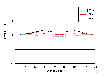 Figure 3. INL vs Tap Position (Rheostat Mode)
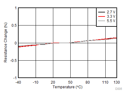 Figure 5. End-to-End RTOTAL Change vs Temperature
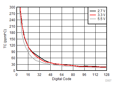 Figure 7. Temperature Coefficient vs TAP Position (Rheostat Mode)
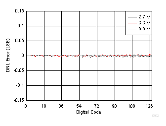 Figure 2. DNL vs Tap Position (Potentiometer Mode)
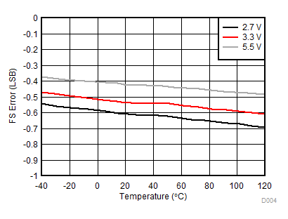 Figure 4. Full Scale Error vs Temperature
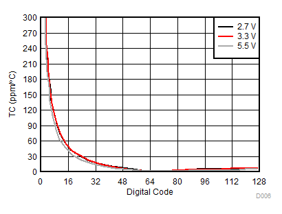 Figure 6. Temperature Coefficient vs TAP Position (Potentiometer Mode)
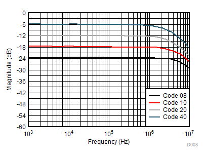 Figure 8. Frequency Response
