SLIS144B September 2011 – February 2017
PRODUCTION DATA.
- 1 Features
- 2 Applications
- 3 Description
- 4 Revision History
- 5 Device Comparison Table
- 6 Pin Configuration and Functions
- 7 Specifications
- 8 Parameter Measurement Information
- 9 Detailed Description
- 10Application and Implementation
- 11Power Supply Recommendations
- 12Layout
- 13Device and Documentation Support
- 14Mechanical, Packaging, and Orderable Information
Package Options
Mechanical Data (Package|Pins)
- DCK|6
Thermal pad, mechanical data (Package|Pins)
- DCK|6
Orderable Information
1 Features
- Single-Channel, 128-Position Resolution
- 10-kΩ End-to-End Resistance Options
- Low Temperature Coefficient: 22 ppm/°C
- I2C Serial Interface
- 2.7-V to 5.5-V Single-Supply Operation
- ±20% Resistance Tolerance
- A and B Versions Have Different I2C Addresses
- L Terminal is Internal and Connected to GND
- Operating Temperature: –40°C to +125°C
- Available in Industry Standard SC70 Packages
- ESD Performance Tested per JESD 22
- 2000-V Human-Body Model (A114-B, Class II)
2 Applications
- Mechanical Potentiometer Replacement
- Adjustable Power Supplies
- Adjustable Gain Amplifiers and Offset Trimming
- Precision Calibration of Setpoint Thresholds
- Sensor Trimming and Calibration
3 Description
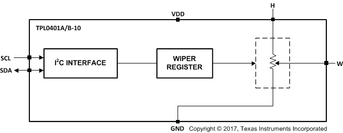
The TPL0401x-10 device is a single-channel, linear-taper digital potentiometer with 128 wiper positions. The TPL0401x-10 has the low terminal internal and connected to GND. The position of the wiper can be adjusted using an I2C interface. The TPL0401x-10 is available in a 6-pin SC70 package with a specified temperature range of –40°C to +125°C. The part has a 10-kΩ end-to-end resistance and can operate with a supply voltage range of 2.7 V to 5.5 V. This kind of product is widely used in setting the voltage reference for low power DDR3 memory.
The TPL0401x-10 has the low terminal internal and connected to GND.
Device Information(1)
| PART NUMBER | PACKAGE | BODY SIZE (NOM) |
|---|---|---|
| TPL0401A-10 TPL0401B-10 |
SC70 (6) | 2.00 mm × 1.25 mm |
- For all available packages, see the orderable addendum at the end of the data sheet.
Simplified Schematic
