SLVSB49F November 2011 – January 2015 TPS22910A , TPS22912C
PRODUCTION DATA.
- 1 Features
- 2 Applications
- 3 Description
- 4 Simplified Schematic
- 5 Revision History
- 6 Device Comparison Table
- 7 Pin Configuration and Functions
-
8 Specifications
- 8.1 Absolute Maximum Ratings
- 8.2 ESD Ratings
- 8.3 Recommended Operating Conditions
- 8.4 Thermal Information
- 8.5 Electrical Characteristics
- 8.6 Switching Characteristics, Typical
- 8.7 Typical DC Characteristics
- 8.8 Typical AC Characteristics, TPS22910A
- 8.9 Typical AC Characteristics, TPS22912C
- 8.10 Typical AC Characteristics, TPS22913B
- 8.11 Typical AC Characteristics, TPS22913C
- 9 Parameter Measurement Information
- 10Detailed Description
- 11Application and Implementation
- 12Power Supply Recommendations
- 13Layout
- 14Device and Documentation Support
- 15Mechanical, Packaging, and Orderable Information
Package Options
Mechanical Data (Package|Pins)
- YZV|4
Thermal pad, mechanical data (Package|Pins)
Orderable Information
10 Detailed Description
10.1 Overview
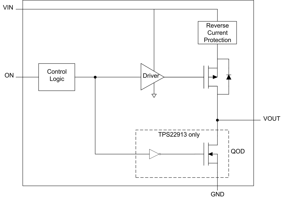
This family of devices are single channel, 2-A load switches in ultra-small, space saving 4-pin WCSP package. These devices implement a low resistance P-channel MOSFET with a controlled rise time for applications that need to limit the inrush current.
These devices are designed to have very low leakage current during off state. This prevents downstream circuits from pulling high standby current from the supply. Integrated control logic, driver, power supply, and output discharge FET eliminates the need for additional external components, which reduces solution size and BOM count.
10.2 Functional Block Diagram
10.3 Feature Description
10.3.1 On/Off Control
The ON pin controls the state of the switch. The ON pin is compatible with standard GPIO logic threshold. It can be used with any microcontroller with 1.2-V, 1.8-V, 2.5-V, 3.3-V, or 5.5-V GPIO.
10.3.2 Under-Voltage Lockout
Under-voltage lockout protection turns off the switch if the input voltage drops below the under-voltage lockout threshold (UVLO). With the ON pin active, the input voltage rising above the under-voltage lockout threshold will cause a controlled turn-on of the switch to limit current over-shoot.
10.3.3 Full-Time Reverse Current Protection
In a scenario where VOUT is greater than VIN, there is potential for reverse current to flow through the pass FET or the body diode. The devices monitor VIN and VOUT voltage levels. When the reverse current voltage threshold (VRCP) is exceeded, the switch is disabled (within 10μs typ). Additionally, the body diode is disengaged so as to prevent any reverse current flow to VIN. The peak instantaneous reverse current is the current it takes to activate the reverse current protection. After the reverse current protection has activated due to the peak instantaneous reverse current, the DC (off-state) leakage current from VOUT and VIN is referred to as IRCP(leak) (see Figure 49). The pass FET, and the output voltage (VOUT), will resume normal operation when the reverse voltage scenario is no longer present.
The following formula can be used to calculate the amount of peak instantaneous reverse current for a particular application:
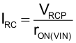
Where,
IRC is the amount of reverse current,
rON(VIN) is the on-resistance at the VIN of the reverse current condition.
VRCP is the reverse voltage threshold.
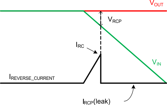 Figure 49. Reverse Current
10.4 Device Functional Modes
Table 2 describes what the VOUT pin will be connected to for a particular device as determined by the ON pin
Table 2. VOUT Function Table
| ON | TPS22910A | TPS22912C | TPS22913B/C |
|---|---|---|---|
| L | VIN | Open | GND |
| H | Open | VIN | VIN |