SLVS832D November 2008 – July 2014 TPS22941 , TPS22942 , TPS22943 , TPS22944 , TPS22945
PRODUCTION DATA.
- 1 Features
- 2 Applications
- 3 Description
- 4 Revision History
- 5 Device Comparison Table
- 6 Pin Configuration and Functions
- 7 Specifications
- 8 Detailed Description
- 9 Application and Implementation
- 10Power Supply Recommendations
- 11Layout
- 12Device and Documentation Support
- 13Mechanical, Packaging, and Orderable Information
Package Options
Mechanical Data (Package|Pins)
- DCK|5
Thermal pad, mechanical data (Package|Pins)
Orderable Information
1 Features
- Input Voltage Range: 1.62 V to 5.5 V
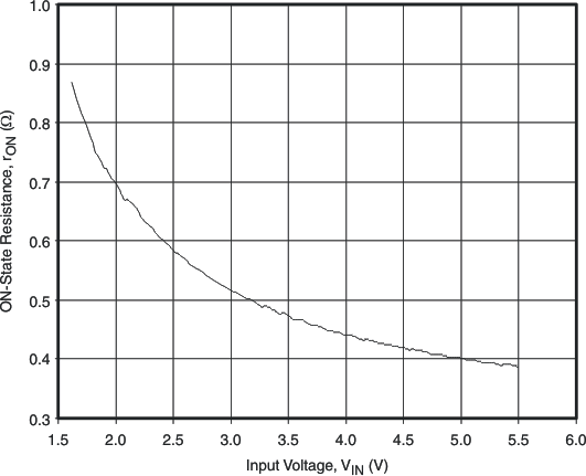
- Low ON resistance
- rON = 0.4 Ω at VIN = 5.5 V
- rON = 0.5 Ω at VIN = 3.3 V
- rON = 0.6 Ω at VIN = 2.5 V
- rON = 0.8 Ω at VIN = 1.8 V
- Minimum Current Limit: 40 mA or 100 mA
- Undervoltage Lockout (UVLO)
- Thermal Shutdown
- Shutdown Current < 1 μA
- Fast Current Limit Response Time
- Fault Blanking
- Auto Restart
- 1.8-V Compatible Control Input Thresholds
- ESD Performance Tested Per JESD 22
- 4000-V Human-Body Model
(A114-B, Class II) - 1000-V Charged-Device Model (C101)
- 4000-V Human-Body Model
- Tiny SC-70 (DCK) Package
- UL Recognized Component (UL File 169910)
- Evaluated to IEC 60950-1, Ed 2, Am1, Annex CC, Test Program 2 with CB Report
2 Applications
- Low-Current Sensor Protection
- HDMI Connector Protection
- Notebooks
- PDAs
- GPS Devices
- MP3 Players
- Peripheral Ports
3 Description
The TPS22941/2/3/4/5 load switches provide protection to systems and loads in high-current conditions. The devices contain a 0.4-Ω current-limited P-channel MOSFET that can operate over an input voltage range of 1.62 V to 5.5 V. Current is prevented from flowing when the MOSFET is off. The switch is controlled by an on/off input (ON), which is capable of interfacing directly with low-voltage control signals. The TPS22941/2/3/4/5 includes thermal shutdown protection that prevents damage to the device when a continuous over-current condition causes excessive heating by turning off the switch.
These devices provide an integrated, robust solution to provide current limiting the output current to a safe level by switching into a constant-current mode when the ouptut load exceeds the current-limit threshold. The OC logic output asserts low during overcurrent, undervoltage, or overtemperature conditions. These additional features make the TPS22941/2/3/4/5 an ideal solution for applications where current limiting is necessary.
This family of devices are available in a SC70-5 (DCK) package. It is characterized for operation over the free-air temperature range of –40°C to 85°C.
Device Information(1)
| PART NUMBER | PACKAGE | BODY SIZE (NOM) |
|---|---|---|
| TPS22941 | SC70 (5) | 2.00mm × 2.10 mm |
| TPS22942 | ||
| TPS22943 | ||
| TPS22944 | ||
| TPS22945 |
- For all available packages, see the orderable addendum at the end of the datasheet.