SLVS832D November 2008 – July 2014 TPS22941 , TPS22942 , TPS22943 , TPS22944 , TPS22945
PRODUCTION DATA.
- 1 Features
- 2 Applications
- 3 Description
- 4 Revision History
- 5 Device Comparison Table
- 6 Pin Configuration and Functions
- 7 Specifications
- 8 Detailed Description
- 9 Application and Implementation
- 10Power Supply Recommendations
- 11Layout
- 12Device and Documentation Support
- 13Mechanical, Packaging, and Orderable Information
Package Options
Mechanical Data (Package|Pins)
- DCK|5
Thermal pad, mechanical data (Package|Pins)
Orderable Information
7 Specifications
7.1 Absolute Maximum Ratings(1)
| MIN | MAX | UNIT | ||||
|---|---|---|---|---|---|---|
| VI | Input voltage range | VIN, VOUT, ON | –0.3 | 6 | V | |
| TJ | Operating junction temperature range | Internally Limited | °C | |||
(1) Stresses beyond those listed under absolute maximum ratings may cause permanent damage to the device. These are stress ratings only, and functional operation of the device at these or any other conditions beyond those indicated under Recommended Operating Conditions is not implied. Exposure to absolute-maximum-rated conditions for extended periods may affect device reliability.
7.2 Handling Ratings
| MIN | MAX | UNIT | |||
|---|---|---|---|---|---|
| Tstg | Storage temperature range | –65 | 150 | °C | |
| VESD | Electrostatic discharge | Human body model (HBM), per ANSI/ESDA/JEDEC JS-001, all pins(1) | –4 | 4 | kV |
| Charged device model (CDM), per JEDEC specification JESD22-C101, all pins(2) | –1 | 1 | |||
(1) JEDEC document JEP155 states that 500-V HBM allows safe manufacturing with a standard ESD control process.
(2) JEDEC document JEP157 states that 250-V CDM allows safe manufacturing with a standard ESD control process.
7.3 Recommended Operating Conditions
Over operating free-air temperature range (unless otherwise noted)| MIN | MAX | UNIT | ||
|---|---|---|---|---|
| VIN | Input voltage | 1.62 | 5.5 | V |
| VOUT | Output voltage | VIN | ||
| TA | Ambient free-air temperature | –40 | 85 | °C |
7.4 Thermal Information
| THERMAL METRIC(1) | TPS22941/2/3/4/5 | UNIT | |
|---|---|---|---|
| DCK | |||
| 5 PINS | |||
| θJA | Junction-to-ambient thermal resistance | 294 | °C/W |
| θJC(top) | Junction-to-case (top) thermal resistance | 59.2 | |
| θJB | Junction-to-board thermal resistance | 95.4 | |
| ψJT | Junction-to-top characterization parameter | 0.7 | |
| ψJB | Junction-to-board characterization parameter | 93.9 | |
| θJC(bot) | Junction-to-case (bottom) thermal resistance | N/A | |
(1) For more information about traditional and new thermal metrics, see the IC Package Thermal Metrics application report, SPRA953.
7.5 Electrical Characteristics
VIN = 1.62 V to 5.5 V, TA = –40°C to 85°C (unless otherwise noted)| PARAMETER | TEST CONDITIONS | TA | MIN | TYP(1) | MAX | UNIT | ||
|---|---|---|---|---|---|---|---|---|
| IIN | Quiescent current | IOUT = 0 mA, | VIN = 1.62 V to 5.5 V | Full | 40 | 80 | μA | |
| IIN(OFF) | OFF-State supply current | VON = 0 V (TPS22943/4/5) or VON = VIN (TPS22941/2) |
VIN = 3.6 V, VOUT open |
Full | 1 | μA | ||
| IOUT(LEAKAGE) | OFF-State switch current | VON = 0 V (TPS22943/4/5) or VON = VIN (TPS22941/2) |
VIN = 3.6 V, VOUT short to GND |
Full | 1 | μA | ||
| rON | ON-state resistance | IOUT = 20 mA | VIN = 5.5 V | 25°C | 0.4 | 0.5 | Ω | |
| Full | 0.6 | |||||||
| VIN = 3.3 V | 25°C | 0.5 | 0.6 | |||||
| Full | 0.7 | |||||||
| VIN = 2.5 V | 25°C | 0.6 | 0.7 | |||||
| Full | 0.8 | |||||||
| VIN = 1.8 V | 25°C | 0.8 | 0.9 | |||||
| Full | 1.1 | |||||||
| VIN = 1.62 V | 25°C | 0.9 | 1.1 | |||||
| Full | 1.2 | |||||||
| ION | ON input leakage current | VON = VIN or GND | Full | 1 | μA | |||
| ILIM | Current limit | VIN = 3.3 V, VOUT = 3 V | TPS22941/3 | Full | 40 | 65 | 80 | mA |
| TPS22942/4/5 | 100 | 150 | 200 | |||||
| TSD | Thermal shutdown | Shutdown threshold | Full | 140 | °C | |||
| Return from shutdown | 130 | |||||||
| Hysteresis | 10 | |||||||
| UVLO | Undervoltage shutdown | VIN increasing | Full | 1.32 | 1.42 | 1.52 | V | |
| Undervoltage shutdown hysteresis | Full | 45 | mV | |||||
| Control Output (OC) | ||||||||
| Vol | OC output logic low voltage | VIN = 5 V, ISINK = 10 mA | Full | 0.1 | 0.2 | V | ||
| VIN = 1.8 V, ISINK = 10 mA | 0.1 | 0.3 | ||||||
| Ioz | OC output high leakage current voltage | VIN = 5 V, Switch ON | Full | 0.5 | μA | |||
| Control Input (ON) | ||||||||
| Vih | ON high-level input voltage | VIN = 1.8 V | Full | 1.1 | V | |||
| VIN = 2.5 V | Full | 1.3 | V | |||||
| VIN = 3.3 V | Full | 1.4 | V | |||||
| VIN = 5.5 V | Full | 1.7 | V | |||||
| Vil | ON low-level input voltage | VIN = 1.8 V | Full | 0.5 | V | |||
| VIN = 2.5 V | Full | 0.7 | V | |||||
| VIN = 3.3 V | Full | 0.8 | V | |||||
| VIN = 5.5 V | Full | 0.9 | V | |||||
| Ii | ON high-level input leakage current | VIN = 1.8 V to 5 V, Switch ON | Full | 1 | μA | |||
(1) Typical values are at VIN = 3.3 V and TA = 25°C.
7.6 Switching Characteristics
VIN = 3.3 V, RL = 500 Ω, CL = 0.1 μF, TA = 25°C (unless otherwise noted)| PARAMETER | TEST CONDITIONS | MIN | TYP | MAX | UNIT | ||
|---|---|---|---|---|---|---|---|
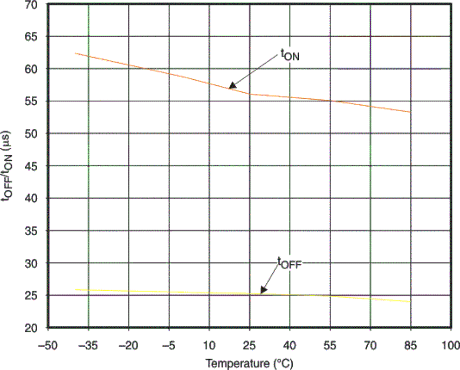
| tON | Turn-ON time | RL = 500 Ω, | CL = 0.1 μF | 60 | μs | ||
| tOFF | Turn-OFF time | RL = 500 Ω, | CL = 0.1 μF | 30 | μs | ||
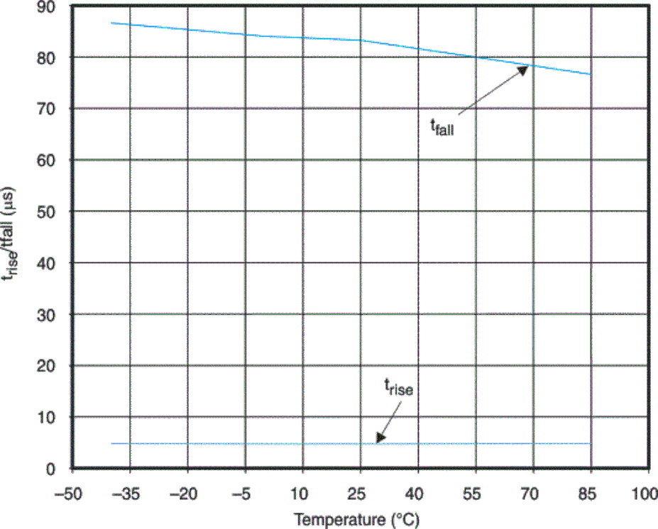
| tr | VOUT rise time | RL = 500 Ω, | CL = 0.1 μF | 10 | μs | ||
| tf | VOUT fall time | RL = 500 Ω, | CL = 0.1 μF | 90 | μs | ||
| tBLANK | Over current blanking time | TPS22941/2/5 | 5 | 10 | 20 | ms | |
| tRSTART | Auto-restart time | TPS22941/2/5 | 40 | 80 | 160 | ms | |
| Short-circuit response time | VIN = VON = 3.3 V, moderate overcurrent condition | 9 | μs | ||||
| VIN = VON = 3.3 V, hard short | 4 | μs | |||||
7.7 Typical Characteristics
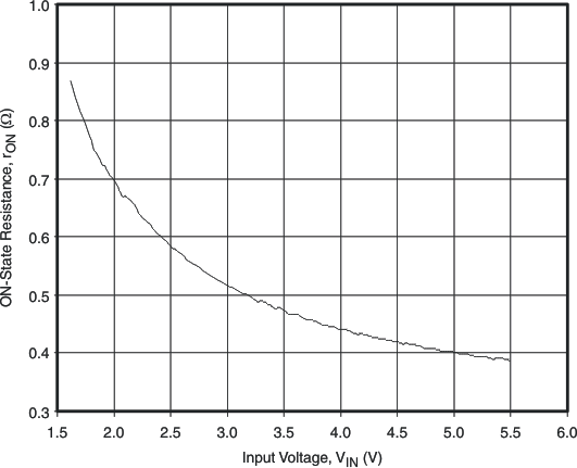 Figure 1. rON vs VIN
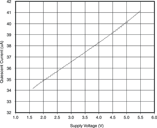 Figure 3. Quiescent Current vs VIN
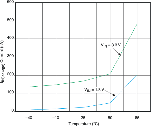 Figure 5. IIN(Leakage) vs Temperature
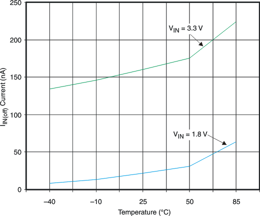 Figure 7. IIN(off) vs Temperature
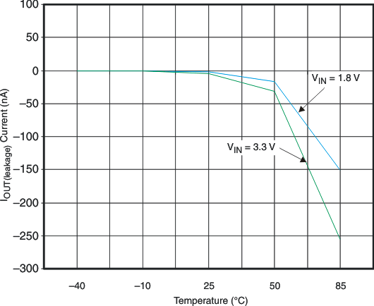 Figure 9. IOUT(leakage) vs Temperature
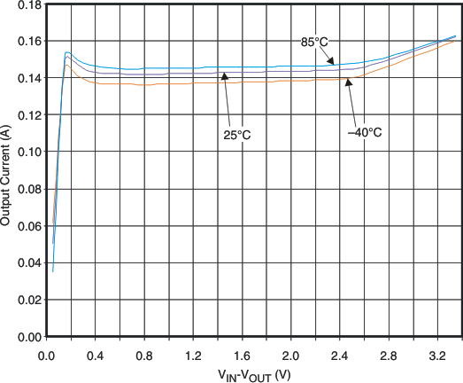 Figure 11. ILIM vs Output Voltage (TPS22942, TPS22944, TPS22945)
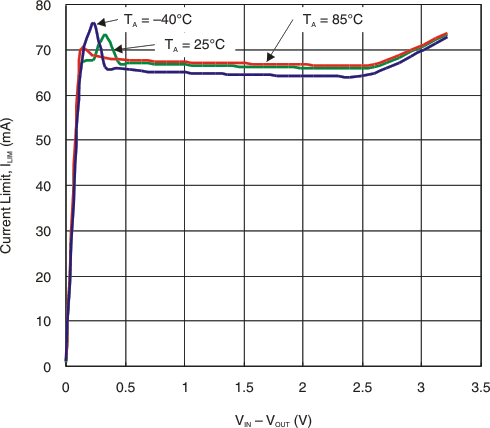 Figure 13. ILIM vs (VIN-VOUT) (TPS22941, TPS22943)
| CL = 0.1 µF | RL = 350 Ω | VIN = 3.3 V |
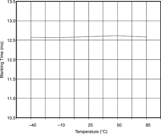 Figure 17. tBLANK vs Temperature (VIN = 3.3 V)
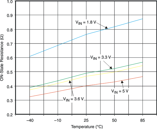 Figure 2. rON vs Temperature
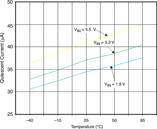 Figure 4. Quiescent Current vs Temperature
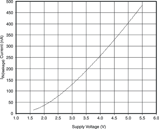 Figure 6. IIN(Leakage) vs VIN
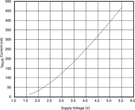 Figure 8. IIN(off) vs VIN
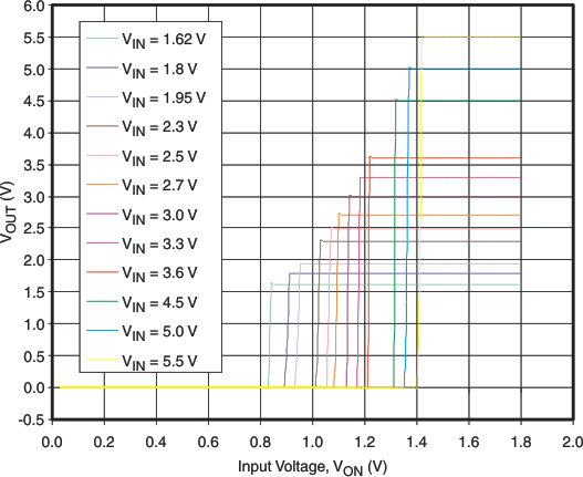 Figure 10. VOUT vs ON Threshold
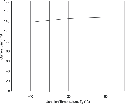 Figure 12. ILIM vs Temperature (TPS22942, TPS22944, TPS22945)
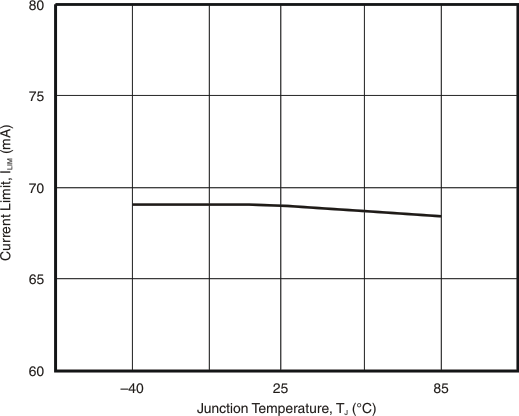 Figure 14. ILIM vs Temperature (TPS22941, TPS22943)
| CL = 0.1 µF | RL = 350 Ω | VIN = 3.3 V |
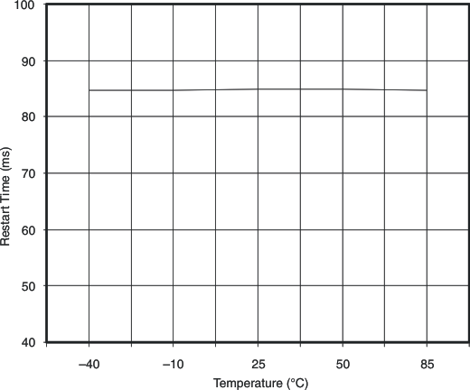 Figure 18. tRESTART vs Temperature (VIN = 3.3 V)