SLVS908D February 2009 – June 2015 TPS22949
PRODUCTION DATA.
- 1 Features
- 2 Applications
- 3 Description
- 4 Revision History
- 5 Description (continued)
- 6 Pin Configuration and Functions
-
7 Specifications
- 7.1 Absolute Maximum Ratings
- 7.2 ESD Ratings
- 7.3 Recommended Operating Conditions
- 7.4 Thermal Information
- 7.5 Electrical Characteristics
- 7.6 Current Limiter Electrical Characteristics
- 7.7 Low-Noise LDO Regulator Electrical Characteristics
- 7.8 Current Limiter Switching Characteristics
- 7.9 Typical Characteristics
- 8 Detailed Description
- 9 Application and Implementation
- 10Power Supply Recommendations
- 11Layout
- 12Device and Documentation Support
- 13Mechanical, Packaging, and Orderable Information
Package Options
Mechanical Data (Package|Pins)
- DRG|8
Thermal pad, mechanical data (Package|Pins)
- DRG|8
Orderable Information
1 Features
- Integrated Current Limiter
- Input Voltage Range: 1.62 V to 4.5 V
- Low ON-Resistance
- rON = 300-mΩ at VIN = 4.5 V
- rON = 350-mΩ at VIN = 3.3 V
- rON = 400-mΩ at VIN = 2.5 V
- rON = 600-mΩ at VIN = 1.8 V
- Integrated 100-mA Minimum Current Limit
- Undervoltage Lockout
- Fast-Current Limit Response Time
- Integrated Fault Blanking and Auto Restart
- Stable Without Current Limiter Output Capacitor (TPS22949A Only)
- Integrated Low-Noise RF LDO
- Input Voltage Range: 1.62 V to 4.5 V
- Low Noise: 50 μVrms (10 Hz to 100 kHz)
- 80-dB VIN PSRR (10 Hz to 10 kHz)
- Fast Start-Up Time: 130 μs
- Low Dropout 100 mV at Iload =100 mA
- Integrated Output Discharge
- Stable With 2.2-μF Output Capacitor
- 1.8-V Compatible Control Input Threshold
- ESD Performance Tested Per JESD 22
- 3500 V Human Body Model
(A114-B, Class II) - 1000 V Charged Device Model
(C101)
- 3500 V Human Body Model
- Tiny 8-Terminal YZP Package (1.9 mm × 0.9 mm, 0.5-mm Pitch, 0.5-mm Height) and WSON-8 (DRG) 3.0 mm × 3.0 mm
2 Applications
- Fingerprint Module Protection
- Portable Consumer Electronics
- Smart Phones
- Notebooks
- Control Access Systems
3 Description
The TPS22949 and TPS22949A are devices that provide protection to systems and loads in high-current conditions. The device contains a 500-mΩ current-limited P-channel MOSFET that can operate over an input voltage range of 1.62 V to 4.5 V as well as a low-dropout (LDO) regulator with a fixed output voltage of 1.8 V.
The switch is controlled by an on/off input (EN1), which can interface directly with low-voltage control signals. When the switch current reaches the maximum limit, the TPS22949/TPS22949A operates in a constant-current mode to prohibit excessive currents from causing damage. If the constant current condition persists after 12 ms, these devices shut off the switch and pull the fault signal pin (OC) low. The TPS22949/TPS22949A has an auto-restart feature that turns the switch on again after 70 ms if the EN1 pin is still active.
The output of the current limiter is internally connected to an RF low-dropout (LDO) regulator that offers good AC performance with very low ground current, good power supply rejection ratio (PSRR), low noise, fast start-up, and excellent line and load transient response. The output of the regulator is stable with ceramic capacitors. This LDO uses a precision voltage reference and feedback loop to achieve overall accuracy of 2% over all load, line, process, and temperature variations.
Device Information(1)
| PART NUMBER | PACKAGE | BODY SIZE (NOM) |
|---|---|---|
| TPS22949 | DSBGA (8) | 1.90 mm × 0.90 mm |
| TPS22949A | 1.90 mm × 0.90 mm | |
| DSBGA (8) | ||
| WSON (8) | 3.00 mm × 3.00 mm |
- For all available packages, see the orderable addendum at the end of the data sheet.
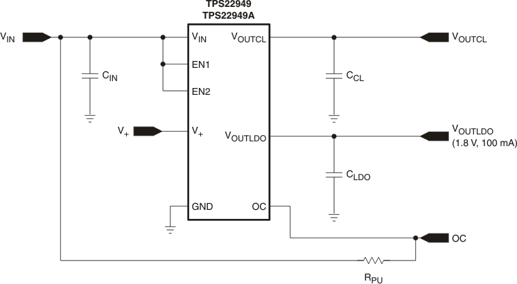
Typical Application Schematic

4 Revision History
Changes from C Revision (January 2010) to D Revision
- Added ESD Ratings table, Feature Description section, Device Functional Modes, Application and Implementation section, Power Supply Recommendations section, Layout section, Device and Documentation Support section, and Mechanical, Packaging, and Orderable Information sectionGo
- Deleted Dissipation Ratings tableGo