SLVSBM6B December 2012 – November 2015 TPS22981
PRODUCTION DATA.
- 1 Features
- 2 Applications
- 3 Description
- 4 Revision History
- 5 Pin Configuration and Functions
- 6 Specifications
- 7 Detailed Description
- 8 Application and Implementation
- 9 Power Supply Recommendations
- 10Layout
- 11Device and Documentation Support
- 12Mechanical, Packaging, and Orderable Information
Package Options
Mechanical Data (Package|Pins)
- RGP|20
Thermal pad, mechanical data (Package|Pins)
- RGP|20
Orderable Information
7 Detailed Description
7.1 Overview
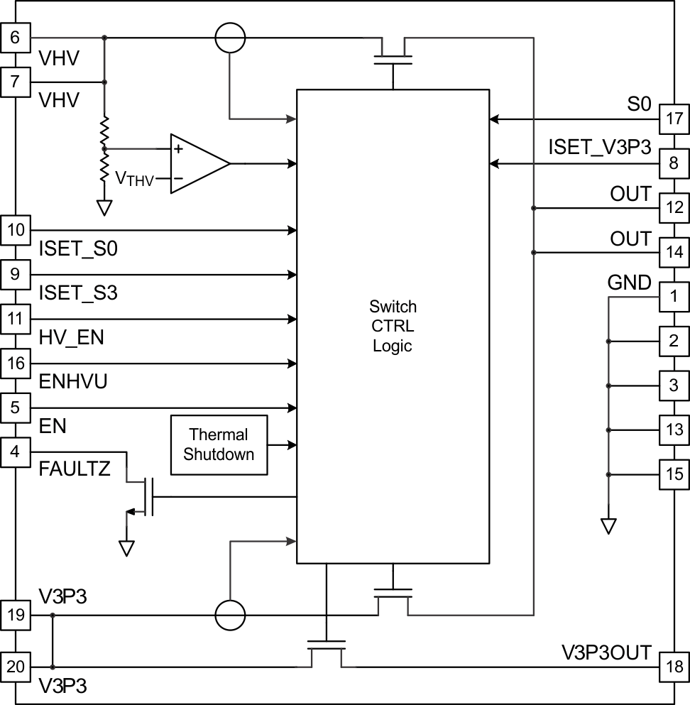
TPS22981 is a power mux designed for Thunderbolt™ and Thunderbolt II™ applications (based on the Mini DisplayPort connector). Thunderbolt and Thunderbolt II provide options for different voltage levels to be supplied to an external Thunderbolt cable, and on to a device or host connected on the far end of that cable. Thunderbolt and Thunderbolt II initiate operation with a nominal 3.3-V voltage (3-V to 3.6-V range is supported by TPS22981), but can be configured through the interface protocol to enable a high-voltage mode (TPS22981 supports the range of 4.5 V to 19.8 V). In operation, transition from the 3.3-V mode to the high-voltage mode requires that system brownout not occur. The TPS22981 achieves this by enabling the high-voltage path (when a high-voltage input is available and HV_EN is asserted) and monitoring for reverse current though the low-voltage switch back to V3P3. When reverse current is detected, the low-voltage path is disabled. Similarly, when switching from high voltage back to low voltage, it is normally undesirable for the system output voltage to brownout. TPS22981 avoids brownout by breaking the high-voltage connection and discharging the output until it reaches approximately 3.3 V, at which point the low-voltage path is enabled to avoid excessive droop of the output voltage. However, if the output voltage (on the OUT pins) is loaded, the output voltage may transition to 0 V before returning to 3.3 V (see Transition Delays).
TPS22981 also provides resistor-controlled current limiting, undervoltage lockout (UVLO), and thermal protection. The high-voltage path on TPS22981 may be current limited to two independently controlled current-limiting levels, with the current-limiting level selected through the S0 input pin. A system host processor may be alerted to fault conditions with the FAULTZ pin (see Table 3).
7.3 Feature Description
7.3.1 Current Limit
Figure 1 shows a simplified view of the TPS22981 current limit function. Both the high-voltage supply current limit and the V3P3 supply current limit are adjustable by external resistors.
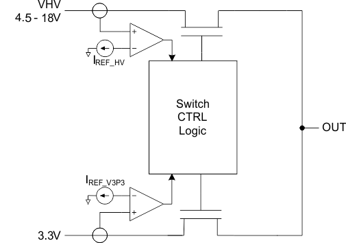 Figure 1. Simplified Current Limit Diagram
The current IREF_HV and IREF_V3P3 that set the current limit threshold are set with three external resistors as shown in Figure 2. When the TPS22981 is passing the V3P3 voltage, the current limit is set by RSET_V3P3. The VHV path has two modes that allow setting two different current limits. The S0 pin determines which current limit is used. When S0 is asserted high, RSET_S0 sets the current limit. When S0 is low, RSET_S3 sets the current limit. This allows the system to have two separate VHV current limits for different modes such as active and sleep.
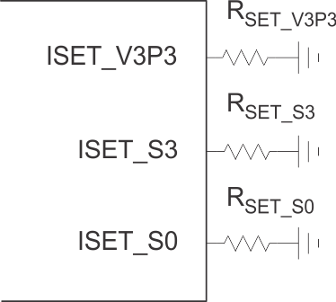 Figure 2. External RSET Resistance to Set Current Limits
7.3.2 Current Limit Threshold
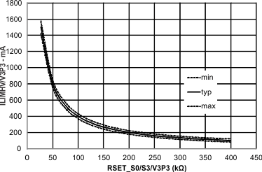 Figure 3. ILIM vs RSET for VHV and V3P3
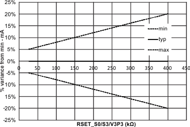 Figure 4. % Variance from Minimum ILIM vs RSET
Figure 3 shows the minimum, typical, and maximum current limit for either supply versus its corresponding RSET value. Equation 1 is used to determine the RSET needed to set a typical ILIM for a given supply and mode. Figure 4 shows the percent variation from the typical ILIM value to the minimum and maximum ILIM values.
SPACE

where
- RSET = external resistor used to set the current limit for V3P3, VHV (S0), or VHV (S3)
- ILIMTYP = typical current limit for V3P3, VHV (S0), or VHV (S3) set by the external RSET resistor.
SPACE
Each resistor is placed between the corresponding ISET pin and GND, as shown in Figure 2, providing a minimum current limit between 100mA and 1.5A. For a given RSET the minimum current limit and the maximum current limit are determined by Equation 2 and Equation 3.
SPACE

SPACE

SPACE
7.3.3 Maximum Current Limit Threshold
The TPS22981 has a maximum current limit ILIMVHVMAX and ILIM3P3MAX. This prevents excessive current in the case of an ISET pin being shorted to ground.
7.3.4 Transition Delays
Output transitions of the TPS22981 voltages are shown in Figure 5. When the device transitions from VHV to V3P3 at the output, the power switches both turn off until the output falls to near the V3P3 voltage. During this time, a discharge current of IDIS pulls OUT down. If a load is also pulling current from OUT, the output will drop to near 0 V due to the switch OFF-time of T3P3OFF.
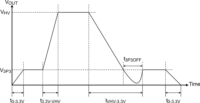 Figure 5. Output Voltage Transitions (Timing Transitions are 10% to > 90%)
7.3.5 Digital Control Signals
The voltage at OUT is controlled by two input digital logic signals, EN and HV_EN. HV_EN controls the state of the VHV switch and EN controls the state of V3P3 switch. Table 1 lists the possible output states given the conditions of the digital logic signals and the device is not in UVLO. See Table 2 for a more complete description including both UVLO conditions.
Table 1. Output State of OUT Given the States EN and HV_EN
| EN | HV_EN | OUT |
|---|---|---|
| 0 | 0 | OPEN |
| 0 | 1 | OPEN |
| 1 | 0 | V3P3 |
| 1 | 1 | VHV |
Figure 6 shows possible combinations of EN and HV_EN controlling OUT of the TPS22981.
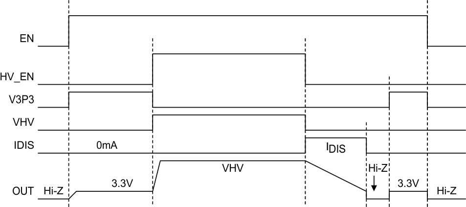 Figure 6. Logic Waveforms Displaying the Transition Between VHV and V3P3
7.3.6 Overcurrent Limit and Short-Circuit Protection
When the load at OUT attempts to draw more current than the limit set by the external RSET resistors for the V3P3 switch and VHV switch (for both S0 and S3 modes), the device will operate in a constant-current mode while lowering the output voltage. Figure 7 shows the delay, tLIM, which occurs from the instance an overcurrent fault is detected until the output current is lowered to ILIMHV tolerances for VHV or ILIM3V3 tolerances for V3P3 shown in Figure 3. Figure 8 shows the response time versus a resistance shorted across the output.
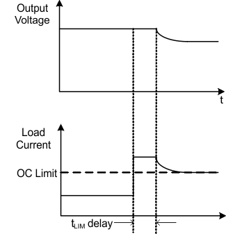 Figure 7. Overcurrent Output Response
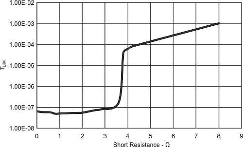 Figure 8. Overcurrent Response Time vs Short Resistance
All short-circuit conditions are treated as overcurrent conditions. In the event of a short circuit, the device will limit the output current to the corresponding RSET value and continue to do so until thermal shutdown is encountered or the short-circuit condition is removed.
7.3.7 Reverse Current Protection
Reverse current protection for the V3P3 supply to OUT triggers at IREV3P3 causing the V3P3 supply switch to open. When the HV_EN signal is not asserted and reverse current protection is triggered, a discharge current source is turned on to bring the output voltage to near the V3P3 voltage.
7.3.8 Reverse Current Blocking
The VHV switch blocks reverse current flow from OUT to VHV when the switch is off.
7.3.9 Thermal Shutdown
The device enters thermal shutdown when junction temperature reaches TSD. The device will resume previous state on power up once the junction temperature has dropped by 10°C. Connect thermal vias to the exposed GND pad underneath the device package for improved thermal diffusion.
7.4 Device Functional Modes
7.4.1 UVLO and Enable
When ENHVU is low, the TPS22981 is enabled by the logical AND of the EN input, the V3P3 UVLO, and the Thermal Shutdown. When the V3P3 UVLO threshold has been crossed, the device is not in thermal shutdown, and the EN input is high, the device will enable. When the V3P3 UVLO triggers, regardless of the states of any digital logic controls, the device will open all switches.
ENHVU adds the VHV UVLO to the logical decision enabling the device. When ENHVU is high, the TPS22981 is enabled by the logical AND of the EN input, the V3P3 UVLO, the VHV UVLO, and the thermal shutdown. When both UVLO thresholds have been crossed, the device is not in thermal shutdown, and the EN input is high, the device will enable. When either UVLO triggers, regardless of the states of any digital logic controls, the device will open all switches. Table 2 shows the pin and voltage configurations for enabling the device.
NOTE
A 1 for the UVLO columns means the device is in a UVLO condition. A PD indicates a pulldown resistance of ROUTDIS to GND.
Table 2. Device Enable Control (When in an Undervoltage Condition, UVLO = 1)
| EN | ENHVU | HV_EN | V3P3 UVLO | VHV UVLO | OUT |
|---|---|---|---|---|---|
| 0 | X | X | X | X | PD |
| 1 | X | X | 1 | X | PD |
| 1 | 1 | X | 0 | X | OPEN |
| 1 | 1 | X | 1 | X | PD |
| 1 | 0 | 0 | 0 | X | V3P3 |
| 1 | 1 | 0 | 0 | 0 | V3P3 |
| 1 | X | 1 | 0 | 0 | VHV |
| 1 | 0 | 1 | 0 | 1 | V3P3 |
7.4.2 FAULTZ Output
The TPS22981 has an open-drain FAULTZ output. When the device is in a fault condition, the FAULTZ output will pull low. Connect FAULTZ through a pullup resistance to V3P3. A Fault occurs during any of the following conditions.
- EN = 1 and V3P3 is in UVLO (device enabled and V3P3 is in an undervoltage condition)
- EN = 1 and in thermal shutdown condition
- EN = 1, HV_EN = 1, and VHV is in UVLO (device enabled, high voltage enabled, and VHV is in an undervoltage condition)
Table 3 shows these conditions and the resulting FAULTZ output. Note, when V3P3 is below the UVLO threshold, FAULTZ will be 0 when EN=1 or 1 when EN=0. However, when V3P3 falls below VFAULTZVAL, the FAULTZ output is unknown.
Table 3. FAULTZ Output Conditions (when in an undervoltage condition, UVLO = 1)
| EN | HV_EN | Thermal Shutdown | V3P3 UVLO | VHV UVLO | FAULTZ (Active Low) |
|---|---|---|---|---|---|
| 0 | X | X | X | X | 1 |
| 1 | X | X | 1 | X | 0 |
| 1 | X | Yes | 0 | X | 0 |
| 1 | 0 | No | 0 | 1 | 1 |
| 1 | 1 | No | 0 | 1 | 0 |
| 1 | X | No | 0 | 0 | 1 |
TI recommends that the pullup resistance on FAULTZ be 100 kΩ and must be greater than or equal to 30 kΩ.
