SLVSCL4B August 2014 – September 2014 TPS22994
PRODUCTION DATA.
- 1 Features
- 2 Applications
- 3 Description
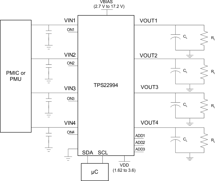
- 4 Simplified Schematic
- 5 Revision History
- 6 Device Comparison Table
- 7 Pin Configuration and Functions
- 8 Specifications
-
9 Detailed Description
- 9.1 Overview
- 9.2 Functional Block Diagram
- 9.3
Feature Description
- 9.3.1 Operating Frequency
- 9.3.2 SDA/SCL Pin Configuration
- 9.3.3 Address (ADDx) Pin Configuration
- 9.3.4 On-Delay Control
- 9.3.5 Slew Rate Control
- 9.3.6 Quick Output Discharge (QOD) Control
- 9.3.7 Mode Registers
- 9.3.8 SwitchALL™ Command
- 9.3.9 VDD Supply For I2C Operation
- 9.3.10 Input Capacitor (Optional)
- 9.3.11 Output Capacitor (Optional)
- 9.3.12 I2C Protocol
- 9.4 Device Functional Modes
- 9.5 Register Map
-
10Applications and Implementation
- 10.1 Application Information
- 10.2 Typical Application
- 11Layout
- 12Device and Documentation Support
- 13Mechanical, Packaging, and Orderable Information
Package Options
Mechanical Data (Package|Pins)
- RUK|20
Thermal pad, mechanical data (Package|Pins)
- RUK|20
Orderable Information
1 Features
- Input Voltage: 1.0 V to 3.6 V
- Low ON-State Resistance (VBIAS = 7.2 V)
- RON = 41 mΩ at VIN = 3.3 V
- RON = 41 mΩ at VIN = 1.8 V
- RON = 41 mΩ at VIN = 1.5 V
- RON = 41 mΩ at VIN = 1.0 V
- VBIAS voltage range: 2.7 V to 17.2 V
- Suitable for 1S/2S/3S/4S Li-ion Battery Topologies
- 1-A Max Continuous Current Per Channel
- Quiescent Current
- Single Channel < 12 µA
- All Four Channels < 22 µA
- Shutdown Current (All Four Channels) < 7 µA
- Four 1.2-V Compatible GPIO Control Inputs
- I2C Configuration (Per Channel)
- On/Off Control
- Programmable Slew Rate Control (5 options)
- Programmable ON-delay (4 options)
- Programmable Output Discharge (4 options)
- I2C SwitchALL™ Command for Multi-channel/Multi-chip Control
- QFN-20 package, 3 mm x 3 mm, 0.75 mm height
2 Applications
- Ultrathin PC
- Notebook PC
- Tablets
- Servers
- All-In-One PC
3 Description
The TPS22994 is a multi-channel, low RON load switch with user programmable features. The device contains four N-channel MOSFETs that can operate over an input voltage range of 1.0 V to 3.6 V. The switch can be controlled by I2C making it ideal for usage with processors that have limited GPIO available. The rise time of the TPS22994 device is internally controlled in order to avoid inrush current. The TPS22994 has five programmable slew rate options, four ON-delay options, and four quick output discharge (QOD) resistance options.
The channels of the device can be controlled via either GPIO or I2C. The default mode of operation is GPIO control through the ONx terminals. The I2C slave address terminals can be tied high or low to assign seven unique device addresses.
The TPS22994 is available in a space-saving RUK package (0.4-mm pitch) and is characterized for operation over the free-air temperature range of –40°C to 85°C.
Device Information(1)
| PART NUMBER | PACKAGE | BODY SIZE (NOM) |
|---|---|---|
| TPS22994 | WQFN (20) | 3.00 mm x 3.00 mm |
- For all available packages, see the orderable addendum at the end of the datasheet.
4 Simplified Schematic