SLUSCD1C June 2017 – November 2018 TPS2373
PRODUCTION DATA.
- 1 Features
- 2 Applications
- 3 Description
- 4 Revision History
- 5 Pin Configuration and Functions
- 6 Specifications
-
7 Detailed Description
- 7.1 Overview
- 7.2 Functional Block Diagram
- 7.3
Feature Description
- 7.3.1 APD Auxiliary Power Detect
- 7.3.2 PG Power Good (Converter Enable) Pin Interface
- 7.3.3 CLSA and CLSB Classification
- 7.3.4 DEN Detection and Enable
- 7.3.5 Internal Pass MOSFET
- 7.3.6 TPH, TPL and BT PSE Type Indicators
- 7.3.7 VC_IN, VC_OUT, UVLO_SEL, and Advanced PWM Startup
- 7.3.8 AMPS_CTL, MPS_DUTY and Automatic MPS
- 7.3.9 VDD Supply Voltage
- 7.3.10 VSS
- 7.3.11 Exposed Thermal PAD
- 7.4
Device Functional Modes
- 7.4.1 PoE Overview
- 7.4.2 Threshold Voltages
- 7.4.3 PoE Startup Sequence
- 7.4.4 Detection
- 7.4.5 Hardware Classification
- 7.4.6 Inrush and Startup
- 7.4.7 Maintain Power Signature
- 7.4.8 Advanced Startup and Converter Operation
- 7.4.9 PD Hotswap Operation
- 7.4.10 Startup and Power Management, PG and TPH, TPL, BT
- 7.4.11 Adapter ORing
- 7.4.12 Using DEN to Disable PoE
- 7.4.13 ORing Challenges
-
8 Application and Implementation
- 8.1 Application Information
- 8.2
Typical Application
- 8.2.1 Design Requirements
- 8.2.2
Detailed Design Requirements
- 8.2.2.1 Input Bridges and Schottky Diodes
- 8.2.2.2 Protection, D1
- 8.2.2.3 Capacitor, C1
- 8.2.2.4 Detection Resistor, RDEN
- 8.2.2.5 Classification Resistors, RCLSA and RCLSB
- 8.2.2.6 APD Pin Divider Network RAPD1, RAPD2
- 8.2.2.7 Opto-isolators for TPH, TPL and BT
- 8.2.2.8 VC Input and Output, CVCIN and CVCOUT
- 8.2.2.9 UVLO Select, UVLO_SEL
- 8.2.2.10 Automatic MPS and MPS Duty Cycle, RMPS and RMPS_DUTY
- 8.2.2.11 Internal Voltage Reference, RREF
- 8.2.3 Application Curves
- 9 Power Supply Recommendations
- 10Layout
- 11Device and Documentation Support
- 12Mechanical, Packaging, and Orderable Information
Package Options
Refer to the PDF data sheet for device specific package drawings
Mechanical Data (Package|Pins)
- RGW|20
Thermal pad, mechanical data (Package|Pins)
Orderable Information
7.4.3 PoE Startup Sequence
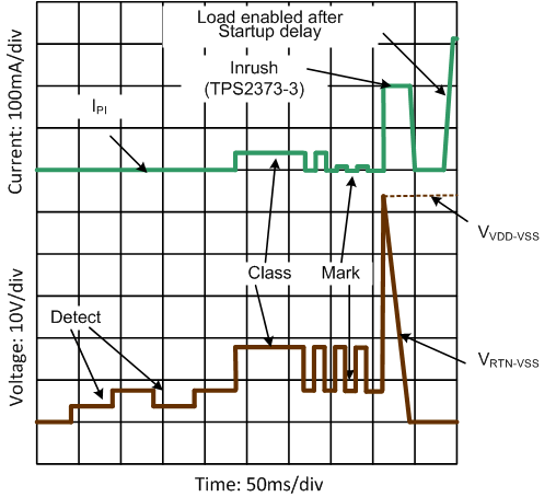
The waveforms of Figure 24 demonstrate detection, classification , and startup from a PSE with Type 3 Class 6 hardware classification. The key waveforms shown are V(VDD-VSS), V(RTN-VSS) and IPI. IEEE 802.3bt requires a PSE allocating Class 6 level of power to generate a minimum of two detection levels, four class and mark cycles, and startup from the fourth mark event. As shown below, the required minimum duration of the first class event has been extended for Type 3 and 4 PSEs. VRTN to VSS falls as the TPS2373 charges CBULK following application of full voltage. In Figure 26, assertion of the PG signal is delayed and used to enable load current as seen in the IPI waveform.
 Figure 24. Startup of Class 6 PD