SLVSCC8A May 2014 – December 2014 TPS2513A-Q1 , TPS2514A-Q1
PRODUCTION DATA.
- 1 Features
- 2 Applications
- 3 Description
- 4 Revision History
- 5 Pin Configuration and Functions
- 6 Specifications
- 7 Detailed Description
- 8 Applications and Implementation
- 9 Power Supply Recommendations
- 10Layout
- 11Device and Documentation Support
Package Options
Mechanical Data (Package|Pins)
- DBV|6
Thermal pad, mechanical data (Package|Pins)
Orderable Information
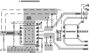
10 Layout
10.1 Layout Guidelines
- For all applications, a 0.1-µF or greater ceramic bypass capacitor between IN and GND is recommended as close to the device as possible for local noise decoupling.
- When USB power switch is used, recommend connect TPS2513A-Q1 and TPS2514A-Q1 IN pin together with USB power switch IN pin. For TPS2513A-Q1, Dual channel USB power switch recommend TPS2561A-Q1, for TPS2514A-Q1, single channel USB power switch recommend TPS2557-Q1.
- Regarding TPS2561A-Q1 layout guidelines, see the TPS2561A-Q1 data sheet (SLVSCC6). Regarding TPS2557-Q1 layout guidelines, see the TPS2557-Q1 data sheet (SLVSC97).
- DP1 and DM1 provide one charging port controller, DP2 and DM2 provide another one charging port controller, when routing the trace, need consider the matching between DP and DM.
10.2 Layout Example