SLVSCC8A May 2014 – December 2014 TPS2513A-Q1 , TPS2514A-Q1
PRODUCTION DATA.
- 1 Features
- 2 Applications
- 3 Description
- 4 Revision History
- 5 Pin Configuration and Functions
- 6 Specifications
- 7 Detailed Description
- 8 Applications and Implementation
- 9 Power Supply Recommendations
- 10Layout
- 11Device and Documentation Support
Package Options
Mechanical Data (Package|Pins)
- DBV|6
Thermal pad, mechanical data (Package|Pins)
Orderable Information
6 Specifications
6.1 Absolute Maximum Ratings(1)
Over recommended junction temperature range, voltages are referenced to GND (unless otherwise noted)| MIN | MAX | UNIT | |||
|---|---|---|---|---|---|
| Voltage range | IN | –0.3 | 7 | V | |
| DP1, DP2 output voltage, DM1, DM2 output voltage | –0.3 | 5.8 | |||
| DP1, DP2 input voltage, DM1, DM2 input voltage | –0.3 | 5.8 | |||
| Continuous output sink current | DP1, DP2 input current, DM1, DM2 input current | 35 | mA | ||
| Continuous output source current | DP1, DP2 output current, DM1, DM2 output current | 35 | mA | ||
| Operating Junction Temperature, TJ | –40 | 125 | °C | ||
| Storage temperature range, Tstg | –65 | 150 | °C | ||
(1) Stresses beyond those listed under Absolute Maximum Ratings may cause permanent damage to the device. These are stress ratings only, and functional operation of the device at these or any other conditions beyond those indicated under Recommended Operating Conditions is not implied. Exposure to absolute-maximum-rated conditions for extended periods may affect device reliability.
6.2 ESD Ratings
| VALUE | UNIT | ||||
|---|---|---|---|---|---|
| V(ESD) | Electrostatic discharge | Human-body model (HBM), per AEC Q100-002(1) | ±2000 | V | |
| Charged-device model (CDM), per AEC Q100-011 | ±750 | ||||
(1) AEC Q100-002 indicates that HBM stressing shall be in accordance with the ANSI/ESDA/JEDEC JS-001 specification.
6.3 Recommended Operating Conditions
Voltages are referenced to GND (unless otherwise noted), positive current are into pins.| MIN | MAX | UNIT | ||
|---|---|---|---|---|
| VIN | Input voltage of IN | 4.5 | 5.5 | V |
| V(DP1) | DP1 data line input voltage | 0 | 5.5 | V |
| V(DM1) | DM1 data line input voltage | 0 | 5.5 | V |
| I(DP1) | Continuous sink or source current | ±10 | mA | |
| I(DM1) | Continuous sink or source current | ±10 | mA | |
| VDP2 | DP2 data line input voltage | 0 | 5.5 | V |
| V(DM2) | DM2 data line input voltage | 0 | 5.5 | V |
| I(DP2) | Continuous sink or source current | ±10 | mA | |
| I(DM2) | Continuous sink or source current | ±10 | mA | |
| TJ | Operating junction temperature | –40 | 125 | °C |
6.4 Thermal Information
| THERMAL METRIC(1) | DBV (6 PINS) | UNITS | |
|---|---|---|---|
| RθJA | Junction-to-ambient thermal resistance | 179.9 | °C/W |
| RθJCtop | Junction-to-case (top) thermal resistance | 117.5 | |
| RθJB | Junction-to-board thermal resistance | 41.9 | |
| ψJT | Junction-to-top characterization parameter | 17.2 | |
| ψJB | Junction-to-board characterization parameter | 41.5 | |
| RθJCbot | Junction-to-case (bottom) thermal resistance | N/A | |
(1) For more information about traditional and new thermal metrics, see the IC Package Thermal Metrics application report, SPRA953.
6.5 Electrical Characteristics
Conditions are –40°C ≤ (TJ = TA) ≤ 125°C, 4.5 V ≤ VIN ≤ 5.5 V. Positive current are into pins. Typical values are at 25°C. All voltages are with respect to GND (unless otherwise noted).| PARAMETER | TEST CONDITIONS | MIN | TYP | MAX | UNIT | |
|---|---|---|---|---|---|---|
| UNDERVOLTAGE LOCKOUT | ||||||
| VUVLO | IN rising UVLO threshold voltage | 3.9 | 4.1 | 4.3 | V | |
| Hysteresis(1) | 100 | mV | ||||
| SUPPLY CURRENT | ||||||
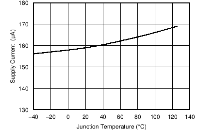
| IIN | IN supply current | 4.5 V ≤ V IN ≤ 5.5 V | 155 | 220 | µA | |
| BC 1.2 DCP MODE (SHORT MODE) | ||||||
| R(DPM_SHORT1) | DP1 and DM1 shorting resistance | VDP1 = 0.8 V, IDM1 = 1 mA | 157 | 200 | Ω | |
| R(DCHG_SHORT1) | Resistance between DP1/DM1 and GND | VDP1 = 0.8 V | 350 | 656 | 1150 | kΩ |
| V(DPL_TH_DETACH1) | Voltage threshold on DP1 under which the device goes back to divider mode | 310 | 330 | 350 | mV | |
| V(DPL_TH_DETACH_HYS1) | Hysteresis(1) | 50 | mV | |||
| R(DPM_SHORT2) | DP2 and DM2 shorting resistance | VDP2 = 0.8V, IDM2 = 1 mA | 157 | 200 | Ω | |
| R(DCHG_SHORT2) | Resistance between DP2/DM2 and GND | VDP2 = 0.8 V | 350 | 656 | 1150 | kΩ |
| V(DPL_TH_DETACH2) | Voltage threshold on DP2 under which the device goes back to divider mode | 310 | 330 | 350 | mV | |
| V(DPL_TH_DETACH_HYS2) | Hysteresis(1) | 50 | mV | |||
| DIVIDER MODE | ||||||
| V(DP1_2.7V) | DP1 output voltage | VIN = 5 V | 2.57 | 2.7 | 2.84 | V |
| V(DM1_2.7V) | DM1 output voltage | VIN = 5 V | 2.57 | 2.7 | 2.84 | V |
| R(DP1_PAD1) | DP1 output impedance | IDP1 = –5 µA | 24 | 30 | 36 | kΩ |
| R(DM1_PAD1) | DM1 output impedance | IDM1 = –5 µA | 24 | 30 | 36 | kΩ |
| V(DP2_2.7V) | DP2 output voltage | VIN = 5 V | 2.57 | 2.7 | 2.84 | V |
| V(DM2_2.7V) | DM2 output voltage | VIN = 5 V | 2.57 | 2.7 | 2.84 | V |
| R(DP2_PAD1) | DP2 output impedance | IDP2 = –5 µA | 24 | 30 | 36 | kΩ |
| R(DM2_PAD1) | DM2 output impedance | IDM2 = –5 µA | 24 | 30 | 36 | kΩ |
| 1.2 V / 1.2 V MODE | ||||||
| V(DP1_1.2V) | DP1 output voltage | VIN = 5 V | 1.12 | 1.2 | 1.28 | V |
| V(DM1_1.2V) | DM1 output voltage | VIN = 5 V | 1.12 | 1.2 | 1.28 | V |
| R(DM1_PAD2) | DP1 output impedance | IDP1 = –5 µA | 80 | 102 | 130 | kΩ |
| R(DP1_PAD2) | DM1 output impedance | IDM1 = –5 µA | 80 | 102 | 130 | kΩ |
| V(DP2_1.2V) | DP2 output voltage | VIN = 5 V | 1.12 | 1.2 | 1.28 | V |
| V(DM2_1.2V) | DM2 output voltage | VIN = 5 V | 1.12 | 1.2 | 1.28 | V |
| R(DP2_PAD2) | DP2 output impedance | IDP2 = –5 µA | 80 | 102 | 130 | kΩ |
| R(DM2_PAD2) | DM2 output impedance | IDM2 = –5 µA | 80 | 102 | 130 | kΩ |
(1) Parameters provided for reference only, and do not constitute part of TI's published device specifications for purposes of TI's product warranty
6.6 Typical Characteristics
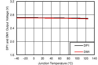
| VIN = 5 V |
| VIN = 5 V |
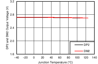
| VIN = 5 V |