SLUSCO9A September 2016 – October 2016 TPS254900-Q1
PRODUCTION DATA.
- 1 Features
- 2 Applications
- 3 Description
- 4 Revision History
- 5 Pin Configuration and Functions
- 6 Specifications
- 7 Parameter Measurement Information
-
8 Detailed Description
- 8.1 Overview
- 8.2 Functional Block Diagram
- 8.3 Feature Description
- 8.4 Device Functional Modes
- 9 Application and Implementation
- 10Power Supply Recommendations
- 11Layout
- 12Device and Documentation Support
- 13Mechanical, Packaging, and Orderable Information
Package Options
Mechanical Data (Package|Pins)
- RVC|20
Thermal pad, mechanical data (Package|Pins)
Orderable Information
1 Features
- AEC-Q100 Qualified With the Following Results:
- Device HBM ESD Classification Level H2
- Device CDM ESD Classification Level C5
- 4.5-V to 6.5-V Input Operating Range
- Integrated 45-mΩ (typ.) High-Side MOSFET
- 3-A Maximum Continuous Output Current
- VBUS ±5% Cable Compensation Accuracy at Connector
- Supports USB BC 1.2 CDP and SDP Modes
- Short-to-Battery Protection on OUT, DP_IN, and DM_IN Pins
- DP_IN and DM_IN IEC 61000-4-2 Rated
- ±8-kV Contact and ±15-kV Air Discharge
- 20-Pin QFN (3-mm × 4-mm) Package
2 Applications
- Automotive USB Charging Ports (Host and Hubs)
- Automotive USB Protection
3 Description
The TPS254900-Q1 device is a USB charging-port controller and power switch with short-to-battery protection. This feature provides protection on OUT, DM_IN and DP_IN. These three pins withstand voltage up to 18 V. The internal MOSFET turns off quickly when the short-to-battery condition occurs. Rapid turnoff is very important to protect the upstream dc-dc converter, processor, or hub data lines.
The TPS254900-Q1 45-mΩ power switch has two selectable, adjustable current limits that support port power management by changing to a lower current limit when adjacent ports are experiencing heavy loads. This is important in systems with multiple ports and upstream power supplies with limited capacity.
The TPS254900-Q1 has a current-sense output that is able to control an upstream supply, which allows it to maintain 5 V at the USB port even with heavy charging currents. This feature is important in systems with long USB cables where significant voltage drops can occur with fast-charging portable devices.
A current monitor allows a system to monitor the load current in real time by monitoring the IMON voltage. The current monitor is very useful and can be used for dynamic port-power management.
The TPS254900-Q1 device also provides ESD protection capability per IEC 61000-4-2, level 4 on DP_IN and DM_IN.
Device Information(1)
| PART NUMBER | PACKAGE | BODY SIZE (NOM) |
|---|---|---|
| TPS254900-Q1 | WQFN (20) | 3.00 mm × 4.00 mm |
- For all available packages, see the orderable addendum at the end of the data sheet.
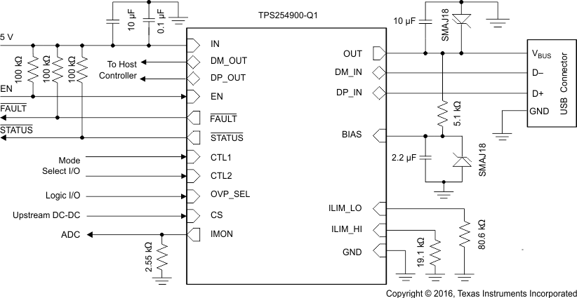
Schematic
