SLVSCC6A March 2014 – June 2014 TPS2561A-Q1
PRODUCTION DATA.
- 1 Features
- 2 Applications
- 3 Description
- 4 Revision History
- 5 Device Comparison Table
- 6 Pin Functions and Configurations
- 7 Specifications
- 8 Parameter Measurement Information
- 9 Detailed Description
-
10Application and Implementation
- 10.1 Application Information
- 10.2
Typical Application
- 10.2.1
Design Current Limit
- 10.2.1.1 Design Requirements
- 10.2.1.2
Detailed Design Procedure
- 10.2.1.2.1 Determine Design Parameters
- 10.2.1.2.2 Programming the Current-Limit Threshold
- 10.2.1.2.3 Designing Above a Minimum Current Limit
- 10.2.1.2.4 Designing Below a Maximum Current Limit
- 10.2.1.2.5 Accounting for Resistor Tolerance
- 10.2.1.2.6 Power Dissipation and Junction Temperature
- 10.2.1.2.7 Auto-Retry Functionality
- 10.2.1.2.8 Two-Level Current-Limit Circuit
- 10.2.2 Application Curves
- 10.2.1
Design Current Limit
- 11Power Supply Requirements
- 12Layout
- 13Device and Documentation Support
- 14Mechanical, Packaging, and Orderable Information
Package Options
Mechanical Data (Package|Pins)
- DRC|10
Thermal pad, mechanical data (Package|Pins)
- DRC|10
Orderable Information
6 Pin Functions and Configurations
DRC PACKAGE
(TOP VIEW)
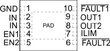
Pin Functions
| PIN | I/O | DESCRIPTION | |
|---|---|---|---|
| NAME | NUMBER | ||
| EN1 | 4 | I | Enable input, logic high turns on channel one power switch |
| EN2 | 5 | I | Enable input, logic high turns on channel two power switch |
| GND | 1 | Ground connection; connect externally to PowerPAD | |
| IN | 2, 3 | I | Input voltage; connect a 0.1 μF or greater ceramic capacitor from IN to GND as close to the IC as possible. |
| FAULT1 | 10 | O | Active-low open-drain output, asserted during overcurrent or overtemperature condition on channel one. |
| FAULT2 | 6 | O | Active-low open-drain output, asserted during overcurrent or overtemperature condition on channel two |
| OUT1 | 9 | O | Power-switch output for channel one |
| OUT2 | 8 | O | Power-switch output for channel two |
| ILIM | 7 | O | External resistor used to set current-limit threshold; recommended 20 kΩ ≤ RILIM ≤ 187 kΩ. |
| PowerPAD™ | PAD | Internally connected to GND; used to heat-sink the part to the circuit board traces. Connect PowerPAD to GND pin externally. | |