SLVSCE1C August 2014 – November 2015 TPS25921A , TPS25921L
PRODUCTION DATA.
- 1 Features
- 2 Applications
- 3 Description
- 4 Application Schematic
- 5 Revision History
- 6 Pin Configuration and Functions
- 7 Specifications
- 8 Parametric Measurement Information
-
9 Detailed Description
- 9.1 Overview
- 9.2 Functional Block Diagram
- 9.3 Feature Description
- 9.4 Device Functional Modes
-
10Applications and Implementation
- 10.1 Application Information
- 10.2
Typical Application
- 10.2.1
Precision Current Limiting and Protection for White Goods
- 10.2.1.1 Design Requirements
- 10.2.1.2 Detailed Design Procedure
- 10.2.1.3 Application Curves
- 10.2.1
Precision Current Limiting and Protection for White Goods
- 10.3 System Examples
- 11Power Supply Recommendations
- 12Layout
- 13Device and Documentation Support
- 14Mechanical, Packaging, and Orderable Information
Package Options
Mechanical Data (Package|Pins)
- D|8
Thermal pad, mechanical data (Package|Pins)
Orderable Information
12 Layout
12.1 Layout Guidelines
- For all applications, a 0.01-uF or greater ceramic decoupling capacitor is recommended between IN terminal and GND. For hot-plug applications, where input power path inductance is negligible, this capacitor can be eliminated/minimized.
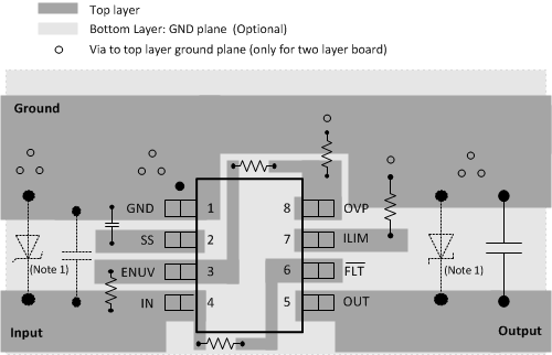
- The optimum placement of decoupling capacitor is closest to the IN and GND terminals of the device. Care must be taken to minimize the loop area formed by the bypass-capacitor connection, the IN terminal, and the GND terminal of the IC. See Figure 52 for a PCB layout example.
- High current carrying power path connections should be as short as possible and should be sized to carry at least twice the full-load current.
- The GND terminal must be tied to the PCB ground plane at the terminal of the IC. The PCB ground should be a copper plane or island on the board.
- Locate all TPS25921x support components: R(ILIM), CSS, and resistors for FLT, ENUV and OVP, close to their connection pin. Connect the other end of the component to the GND pin of the device with shortest trace length.
- The trace routing for the RILIM and CSS components to the device should be as short as possible to reduce parasitic effects on the current limit and soft start timing. These traces should not have any coupling to switching signals on the board.
- OVP and ENUV signal traces should be routed with sufficient spacing from FLT signal trace, to avoid spurious coupling of FLT switching, during fault conditions.
- Protection devices such as TVS, snubbers, capacitors, or diodes should be placed physically close to the device they are intended to protect, and routed with short traces to reduce inductance. For example, a protection Schottky diode is recommended to address negative transients due to switching of inductive loads, and it should be physically close to the OUT pins.
- Obtaining acceptable performance with alternate layout schemes is possible; however this layout has been shown to produce good results and is intended as a guideline.
12.2 Layout Example

1. Optional: Needed only to suppress the transients caused by inductive load switching.
Figure 52. Board Layout