SLVSCQ3B August   2015  – June 2016

PRODUCTION DATA.  

  1. Features
  2. Applications
  3. Description
  4. Revision History
  5. Device Comparison Table
  6. Pin Configuration and Functions
  7. Specifications
    1. 7.1 Absolute Maximum Ratings
    2. 7.2 ESD Ratings
    3. 7.3 Recommended Operating Conditions
    4. 7.4 Thermal Information
    5. 7.5 Electrical Characteristics
    6. 7.6 Timing Requirements
    7. 7.7 Typical Characteristics
  8. Detailed Description
    1. 8.1 Overview
    2. 8.2 Functional Block Diagram
    3. 8.3 Feature Description
      1. 8.3.1 GND
      2. 8.3.2 VIN
      3. 8.3.3 dV/dT
      4. 8.3.4 EN/UVLO
      5. 8.3.5 ILIM
    4. 8.4 Device Functional Modes
  9. Application and Implementation
    1. 9.1 Application Information
    2. 9.2 Typical Application
      1. 9.2.1 Design Requirements
      2. 9.2.2 Detailed Design Procedure
        1. 9.2.2.1 Programming the Current-Limit Threshold: RILIM Selection
        2. 9.2.2.2 Undervoltage Lockout Set Point
        3. 9.2.2.3 Setting Output Voltage Ramp Time (TdVdT)
          1. 9.2.2.3.1 Case 1: Start-Up without Load: Only Output Capacitance COUT Draws Current During Start-Up
          2. 9.2.2.3.2 Case 2: Start-Up with Load: Output Capacitance COUT and Load Draws Current During Start-Up
        4. 9.2.2.4 Support Component Selection—CVIN
      3. 9.2.3 Application Curves
  10. 10Power Supply Recommendations
    1. 10.1 Transient Protection
    2. 10.2 Output Short-Circuit Measurements
  11. 11Layout
    1. 11.1 Layout Guidelines
    2. 11.2 Layout Example
  12. 12Device and Documentation Support
    1. 12.1 Device Support
      1. 12.1.1 Third-Party Products Disclaimer
    2. 12.2 Documentation Support
      1. 12.2.1 Related Documentation
    3. 12.3 Related Links
    4. 12.4 Receiving Notification of Documentation Updates
    5. 12.5 Community Resources
    6. 12.6 Trademarks
    7. 12.7 Electrostatic Discharge Caution
    8. 12.8 Glossary
  13. 13Mechanical, Packaging, and Orderable Information

Package Options

Mechanical Data (Package|Pins)
Thermal pad, mechanical data (Package|Pins)
Orderable Information

6 Pin Configuration and Functions

DRC Package
10-Pin VSON
Top View
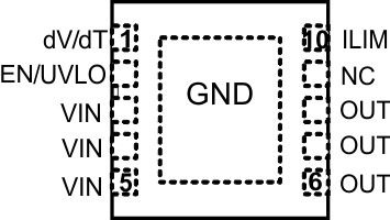
TPS259250 TPS259251 TPS259260 TPS259261 pin_out_top_SLVSCQ3.gif

Pin Functions

PIN TYPE DESCRIPTION
No. NAME
1 dV/dT O Connect a capacitor from this pin to GND to control the ramp rate of OUT voltage at device turnon
2 EN/UVLO I This is a dual function control pin. When used as an ENABLE pin and pulled down, it shuts off the internal pass MOSFET. When pulled high, it enables the device
As an UVLO pin, it can be used to program different UVLO trip point via external resistor divider
3 VIN I Input supply voltage
4
5
6 OUT O Output of the device
7
8
9 NC NC Not Connected Internally. Can be left floating or grounded
10 ILIM O A resistor from this pin to GND sets the overload and short circuit limit
Thermal Pad GND Ground GND