SLVSDG2G July 2016 – December 2019 TPS2660
PRODUCTION DATA.
- 1 Features
- 2 Applications
- 3 Description
- 4 Revision History
- 5 Device Comparison Table
- 6 Pin Configuration and Functions
- 7 Specifications
- 8 Parameter Measurement Information
-
9 Detailed Description
- 9.1 Overview
- 9.2 Functional Block Diagram
- 9.3
Feature Description
- 9.3.1 Undervoltage Lockout (UVLO)
- 9.3.2 Overvoltage Protection (OVP)
- 9.3.3 Reverse Input Supply Protection
- 9.3.4 Hot Plug-In and In-Rush Current Control
- 9.3.5 Overload and Short Circuit Protection
- 9.4 Device Functional Modes
-
10Application and Implementation
- 10.1 Application Information
- 10.2
Typical Application
- 10.2.1 Design Requirements
- 10.2.2 Detailed Design Procedure
- 10.2.3 Application Curves
- 10.3 System Examples
- 10.4 Do's and Don'ts
- 11Power Supply Recommendations
- 12Layout
- 13Device and Documentation Support
- 14Mechanical, Packaging, and Orderable Information
- 14Mechanical, Packaging, and Orderable Information
Package Options
Refer to the PDF data sheet for device specific package drawings
Mechanical Data (Package|Pins)
- RHF|24
- PWP|16
Thermal pad, mechanical data (Package|Pins)
- PWP|16
Orderable Information
9.3.4 Hot Plug-In and In-Rush Current Control
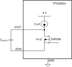
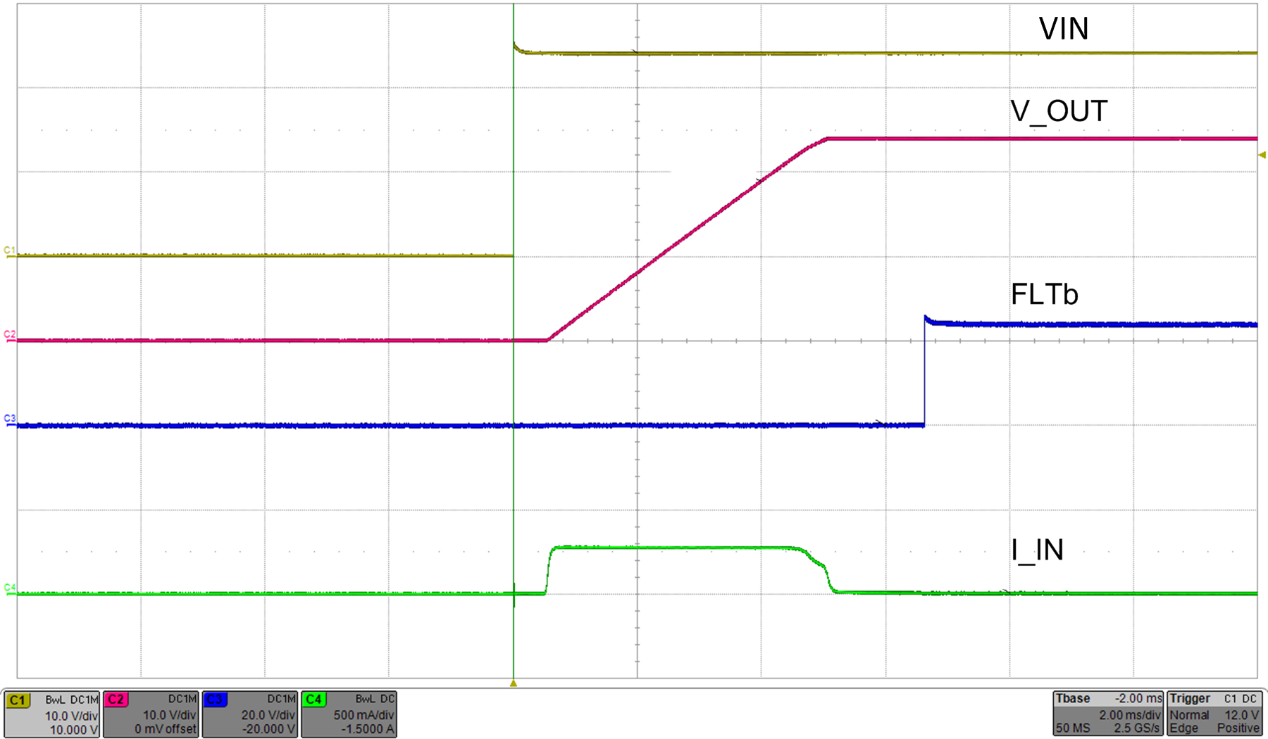
The devices are designed to control the in-rush current upon insertion of a card into a live backplane or other "hot" power source. This limits the voltage sag on the backplane’s supply voltage and prevents unintended resets of the system power. The controlled start-up also helps to eliminate conductive and radiative interferences. An external capacitor connected from the dVdT pin to RTN defines the slew rate of the output voltage at power-on as shown in Figure 37 and Figure 38.
 Figure 37. Output Ramp Up Time tdVdT is Set by C(dVdT)
 The dVdT pin can be left floating to obtain a predetermined slew rate (tdVdT) on the output. When the terminal is left floating, the devices set an internal output voltage ramp rate of 23.9 V/1.6 ms. A capacitor can be connected from dVdT pin to RTN to program the output voltage slew rate slower than 23.9 V/1.6 ms. Use Equation 1 and Equation 2 to calculate the external C(dVdT) capacitance.
Equation 1 governs slew rate at start-up.

where
- I(dVdT) = 4.7 µA (typical)

- Gain(dVdT) = dVdT to VOUT gain = 24.6
The total ramp time (tdVdT) of V(OUT) for 0 to V(IN) can be calculated using Equation 2.

| CdVdT = 22 nF | COUT = 47 µF | RILIM = 5.36 kΩ |