SLVSBE9E April 2012 – June 2015 TPS27081A
PRODUCTION DATA.
- 1 Features
- 2 Applications
- 3 Description
- 4 Revision History
- 5 Pin Configuration and Functions
- 6 Specifications
- 7 Detailed Description
-
8 Application and Implementation
- 8.1 Application Information
- 8.2 Typical Application
- 8.3
System Examples
- 8.3.1 Standby Power Isolation
- 8.3.2 Boost Regulator With True Shutdown
- 8.3.3 Single Module Multiple Power Supply Sequencing
- 8.3.4 Multiple Modules Interdependent Power Supply Sequencing
- 8.3.5 TFT LCD Module Inrush Current Control
- 8.3.6 Multiple Modules Interdependent Supply Sequencing Without a GPIO Input
- 9 Power Supply Recommendations
- 10Layout
- 11Device and Documentation Support
- 12Mechanical, Packaging, and Orderable Information
Package Options
Mechanical Data (Package|Pins)
- DDC|6
Thermal pad, mechanical data (Package|Pins)
Orderable Information
8 Application and Implementation
NOTE
Information in the following applications sections is not part of the TI component specification, and TI does not warrant its accuracy or completeness. TI’s customers are responsible for determining suitability of components for their purposes. Customers should validate and test their design implementation to confirm system functionality.
8.1 Application Information
This section highlights some of the design considerations when implementing this device in various applications.
8.2 Typical Application
8.2.1 Standard Load Switching Application
The TPS27081A device is a high-side load switch that integrates a power PFET and a control NMOS in a tiny package. The device internal components are rated for up to 8-V supply and support up to 3 A of load current. The device can be used in a variety applications. Figure 13 shows a general application of the TPS27081A device to control the load inrush current.
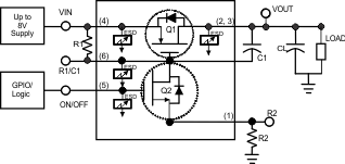 Figure 13. Standard Application Diagram
8.2.1.1 Design Requirements
8.2.1.2 Detailed Design Procedure
8.2.1.2.1 Configuring Q1 ON Resistance
The VGS(Q1) gate-to-source voltage across the PMOS transistor Q1 sets its ON-resistance RQ1(on). Directly connecting the pin R2 to ground maximizes the ON state VGS(Q1) and thus minimizes the VIN to VOUT voltage dropout. Equation 1 describes the VGS(Q1) when a resistor R2 is installed to control the turnon slew rate.

For example,when RR1 = 10 × RR2 and VVIN = 5 V, VGS(Q1) = –4.5 V
NOTE
TI recommends maintaining RR1 > 10 × RR2. The higher value of resistor R1 minimizes quiescent current when PMOS is on, however, the higher value may adversely impact OFF-state leakage current. Refer to the load current (ILOAD) specifications in the Electrical Characteristics table.
8.2.1.2.2 Configuring Turnon Slew Rate
Switching a large capacitive load CLOAD instantaneously results in a load inrush current given by Equation 2.

where
- VOUT(SR) is the output voltage slew rate
An uncontrolled fast rising ON/OFF logic input may result in a high slew rate at the output resulting in a very high dv/dt, thus, leading to a higher inrush current. To control the inrush current, connect a resistor R2 and a capacitor C1 as shown in Figure 13. Use the following equation to configure the TPS27081A slew rate to a specific value. Refer to Table 2 for component values to configure TPS27081A to achieve standard slew rates.

where
- tRISE is the time delta starting from the rising edge of the ON/OFF signal to charge up the load capacitor CLOAD from 10% to 90% of VIN voltage.
NOTE
Equation 3 is accurate to within ±20% across full VIN range supported by TPS27081A. Ensure that R1 > 10 × R2.
Table 2. Component Values for VOUT Rise Time
| CC1 | RISE TIME (µs)(1)(2) | |||||||
|---|---|---|---|---|---|---|---|---|
| RR1 = 10 kΩ, RR2 = 1 kΩ | RR1 = 5.1 kΩ, RR2 = 510 Ω | |||||||
| VVIN (V) | VVIN (V) | |||||||
| 7 | 5 | 3.3 | 1.2 | 7 | 5 | 3.3 | 1.2 | |
| 220 pF | 0.253 | 0.316 | 0.416 | 0.810 | 0.129 | 0.161 | 0.212 | 0.413 |
| 1000 pF | 1.15 | 1.44 | 1.89 | 3.68 | .586 | .732 | .963 | 1.88 |
| 4700 pF | 5.4 | 6.75 | 8.88 | 17.3 | 2.76 | 3.44 | 4.53 | 8.83 |
| 0.18 µF | 207 | 258 | 340 | 663 | 106 | 132 | 173 | 338 |
| 0.27 µF | 310 | 388 | 510 | 994 | 158 | 198 | 260 | 507 |
| 0.33 µF | 379 | 474 | 623 | 1220 | 194 | 242 | 318 | 620 |
| 1 µF | 1150 | 1440 | 1890 | 3680 | 586 | 732 | 963 | 1880 |
8.2.1.2.3 Configuring Turnoff Delay
TPS27081A PMOS turnoff delay from the falling edge of ON/OFF logic signal depends upon the component values of resistor R1 and capacitor C1. Lower values of resistor R1 ensures quicker turnoff.
8.2.1.2.4 Low Voltage ON/OFF Interface
The VGS(Q2) is set by the ON/OFF logic level. To turn ON, the transistor Q2 requires a VGS > 1.0 V (typical). For reliable operation, apply ON/OFF logic following the high-level input voltage (VIH) and low-level input voltage (VIL) limits expressed in Equation 5 and Equation 6.
Minimizing IQ2 × R2 drop helps achieve a direct interface with a low voltage ON/OFF logic. To minimize IQ2 × R2 voltage drop, select a high R1 and R2 ratio. For example, when VVIN = 1.8 V, selecting R1 and R2 = 40 requires VIH > 1 + 45 mV and thus allowing a 1.2-V GPIO interface.
In applications where ON/OFF signal is not available, connect ON/OFF pin to VIN. The TPS27081A turns ON/OFF in sync with the input supply connected to the VIN pin.
NOTE
Connect a pulldown resistor between ON/OFF pin to GND when ON/OFF is driven by a high-impedance (tri-state) driver.
8.2.1.2.5 ON-Chip Power Dissipation
Use Equation 7 to calculate TPS27081A ON-chip power dissipation PD:
where
- IDQ1 and IDQ2 are the DC current flowing through the transistors Q1 and Q2, respectively.
Refer to Electrical Characteristics and/or Figure 1 through Figure 7 to estimate RQ1(on) and RQ2(on) for various values of VGS(Q1) and VGS(Q2), respectively.
NOTE
MOS switches can get extremely hot when operated in saturation region. As a general guideline, to avoid transistors Q1 and Q2 going into saturation region, set VGS > VT + VDS. For example, VGS > 1.5 V and VDS < 200 mV ensures operation as a switch.
8.2.1.3 Application Curves
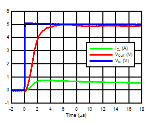
| CC1 = 330 pF |
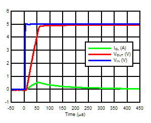
| CC1 = 33 nF |
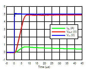
| CC1 = 3300 pF |
8.3 System Examples
8.3.1 Standby Power Isolation
Many applications have some always ON modules to support various core functions. However, some modules are selectively powered ON or OFF to save power and multiplexing of various on board resources. Such modules that are selectively turned ON or OFF require standby power generation. In such applications TPS27081A requires only a single pull-up resistor. In the configuration shown in Figure 17, the VOUT voltage rise time is approximately 250 ns when VVIN = 5 V.
 Figure 17. Standby Power Generation Using TPS27081A
8.3.2 Boost Regulator With True Shutdown
The most common boost regulator topology provides a current leakage path through inductor and diode into the feedback resistor even when the regulator shuts down. Adding a TPS27081A device in the input-side power path prevents this leakage current and thus providing a true shutdown, as shown in Figure 18.
LCD panels require inrush current control to prevent permanent system damages during turnon and turnoff events.
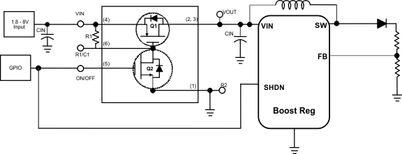 Figure 18. True Shutdown Using TPS27081A
8.3.3 Single Module Multiple Power Supply Sequencing
Most modern SOCs and CPUs require multiple voltage inputs for its analog cores, digital cores, and I/O interfaces. These devices require that these supplies be applied simultaneously or in a certain sequence. The TPS27081A device, when configured as shown in Figure 19 with the VOUT1 rise time adjusted appropriately through resistor R2 and capacitor C1, delays the early arriving LDO output to match up with late-arriving DC-DC output and thus, achieving power sequencing.
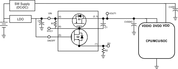 Figure 19. Power Sequencing Using TPS27081A
8.3.4 Multiple Modules Interdependent Power Supply Sequencing
For system integrity reasons, a certain power sequencing may be required among various modules. As shown in Figure 20, Module 2 powers up only after Module 1 is powered up and the Module 1 GPIO output is enabled to turn ON Module 2. The TPS27081A device, when used as shown in this example does not only sequence the Module 2 power, but it also helps prevent inrush current into the power path of Module 1 and 2.
 Figure 20. Power Sequencing Using TPS27081A
8.3.5 TFT LCD Module Inrush Current Control
As shown in Figure 21, LCD panels require inrush current control to prevent permanent system damages during turnon and turnoff events.
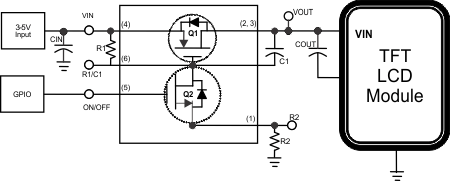 Figure 21. Inrush Current Control Using TPS27081A
8.3.6 Multiple Modules Interdependent Supply Sequencing Without a GPIO Input
When a GPIO signal is not available, connecting the ON/OFF pin of the TPS27081 device as connected to Module 2 powers up Module 2 after poweing up Module 1 when the values for resistor R4 and capacitor C1 are chosen appropriately. The two TPS27081A in this configuration as shown in Figure 22 can control load inrush current.
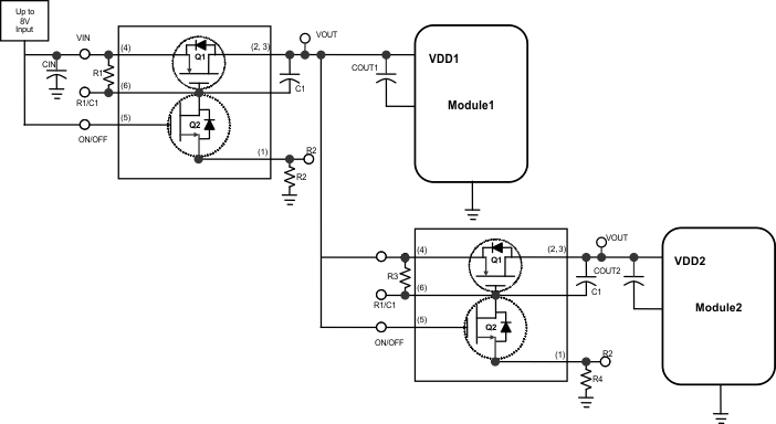 Figure 22. Power Sequencing Using TPS27081A