SLVSBE9E April 2012 – June 2015 TPS27081A
PRODUCTION DATA.
- 1 Features
- 2 Applications
- 3 Description
- 4 Revision History
- 5 Pin Configuration and Functions
- 6 Specifications
- 7 Detailed Description
-
8 Application and Implementation
- 8.1 Application Information
- 8.2 Typical Application
- 8.3
System Examples
- 8.3.1 Standby Power Isolation
- 8.3.2 Boost Regulator With True Shutdown
- 8.3.3 Single Module Multiple Power Supply Sequencing
- 8.3.4 Multiple Modules Interdependent Power Supply Sequencing
- 8.3.5 TFT LCD Module Inrush Current Control
- 8.3.6 Multiple Modules Interdependent Supply Sequencing Without a GPIO Input
- 9 Power Supply Recommendations
- 10Layout
- 11Device and Documentation Support
- 12Mechanical, Packaging, and Orderable Information
Package Options
Mechanical Data (Package|Pins)
- DDC|6
Thermal pad, mechanical data (Package|Pins)
Orderable Information
6 Specifications
6.1 Absolute Maximum Ratings
Specified at TJ = –40°C to 105°C unless otherwise noted.(1)(5)| MIN | MAX | UNIT | ||
|---|---|---|---|---|
| VIN(max) | VIN pin maximum voltage with reference to pin R2 | –0.1 | 8 | V |
| VOUT(max) | VOUT pin maximum voltage with reference to pin R2 | –0.1 | 8 | V |
| VON/OFF | ON/OFF in maximum voltage with respect to pin R2 | –0.3 | 8 | V |
| IQ1(on) | Maximum continuous drain current of Q1 at TJ = 105°C | 3 | A | |
| Maximum pulsed drain current of Q1 (2) at TJ = 105°C | 9.5 | |||
| PD | Maximum power dissipation at TA = 25°C, TJ = 150°C, RθJA = 105°C/W | 1190 | mW | |
| TA | Operating free-air ambient temperature | –40 | 85(4) | °C |
| TJ(max)(3) | Operating virtual junction temperature | 150 | °C | |
| Tstg | Storage temperature | –65 | 150 | °C |
(1) Stresses beyond those listed under Absolute Maximum Ratings may cause permanent damage to the device. These are stress ratings only, which do not imply functional operation of the device at these or any other conditions beyond those indicated under Recommended Operating Conditions. Exposure to absolute-maximum-rated conditions for extended periods may affect device reliability.
(2) Pulse width <300 µs, duty cycle < 2%
(3) Operating at the absolute TJ(max) = 150°C can affect reliability. For higher reliability,TI recommends maintaining TJ < 105°C.
(4) TJ(max) limits and other related conditions apply. Refer to SOA charts, Figure 8 through Figure 12.
(5) Refer to TI’s design support web page at www.ti.com/thermal for improving device thermal performance.
6.2 ESD Ratings
| VALUE | UNIT | |||
|---|---|---|---|---|
| V(ESD) | Electrostatic discharge | Human body model (HBM), per ANSI/ESDA/JEDEC JS-001, all pins(1) | ±2000 | V |
| Charged device model (CDM), per JEDEC specification JESD22-C101, all pins(2) | ±500 | |||
(1) JEDEC document JEP155 states that 500-V HBM allows safe manufacturing with a standard ESD control process.
(2) JEDEC document JEP157 states that 250-V CDM allows safe manufacturing with a standard ESD control process.
6.3 Recommended Operating Conditions
over operating free-air temperature range (unless otherwise noted)| MIN | NOM | MAX | UNIT | ||
|---|---|---|---|---|---|
| VIN | Input voltage | 1 | 8 | V | |
| TA | Operating free-air ambient temperature | –40 | 85 | °C | |
| TJ | Junction temperature | –40 | 105 | °C | |
6.4 Thermal Information
| THERMAL METRIC(1) | TPS27081A | UNIT | |
|---|---|---|---|
| DDC (SOT) | |||
| 6 PINS | |||
| RθJA | Junction-to-ambient thermal resistance | 105 | °C/W |
| RθJC(top) | Junction-to-case (top) thermal resistance | 43 | °C/W |
| RθJB | Junction-to-board thermal resistance | 17.8 | °C/W |
| ψJT | Junction-to-top characterization parameter | 6.5 | °C/W |
| ψJB | Junction-to-board characterization parameter | 16.2 | °C/W |
| RθJC(bot) | Junction-to-case (bottom) thermal resistance | n/a | °C/W |
(1) For more information about traditional and new thermal metrics, see the Semiconductor and IC Package Thermal Metrics application report, SPRA953.
6.5 Electrical Characteristics
Specified over the recommended junction temperature range TJ = –40°C to 105°C unless otherwise noted. Typical values specified at TA = TJ = 25°C.| PARAMETER | TEST CONDITIONS | MIN | TYP | MAX | UNIT | ||
|---|---|---|---|---|---|---|---|
| OFF-TIME CHARACTERISTICS | |||||||
| BVIN1 | Q1 drain-to-source breakdown voltage | VON/OFF = 0 V, VGS(Q1) = 0 V, ID(Q1) = 250 µA | –8 | V | |||
| ILOAD(5) | VIN pin total leakage current | VIN = 8 V, VON/OFF = 0 V, RR1 = 10 kΩ | TJ = 25°C | 0.15 | 0.75 | µA | |
| TJ = 85°C(3) | 5 | 20 | |||||
| VIN = 5 V, VON/OFF = 0 V, RR1 = 10 kΩ | TJ = 25°C | 0.05 | |||||
| TJ = 85°C(3) | 2 | ||||||
| IFQ2 | Q2 drain-to-source leakage current | VIN = 8 V, VON/OFF = 0 V | TJ = 25°C | 0.03 | 0.05 | µA | |
| TJ = 85°C(3) | 0.35 | 0.6 | |||||
| VIN = 5 V, VON/OFF = 0 V | TJ = 25°C | 0.025 | µA | ||||
| TJ = 85°C(3) | 0.25 | ||||||
| ON-TIME CHARACTERISTICS(1) | |||||||
| VIL | ON/OFF pin low-level input voltage | VIN = 5 V, ID(Q1) < 2 µA, RR1 = 10 kΩ, RR2 = RL = 0 Ω | TJ = 25°C | 0.3 | V | ||
| VIN = 5 V, ID(Q1) < 20 µA, RR1 = 10 kΩ, RR2 = RL = 0 Ω |
TJ = 85°C(3) | 0.2 | |||||
| VIH | ON/OFF pin high-level input voltage | VIN = 5 V, RR1 = 10 kΩ | 1 | V | |||
| RQ1(on) | Q1 Channel ON-resistance(4) | VGS = –4.5 V, ID(Q1) = 3 A | 32 | 55 | mΩ | ||
| VGS = –3 V, ID(Q1) = 2.5 A | 44 | 77 | |||||
| VGS = –2.5 V, ID(Q1) = 2.5 A | 50 | 85 | |||||
| VGS = –1.8 V, ID(Q1) = 2 A | 82 | 147 | |||||
| VGS = –1.5 V, ID(Q1) = 1 A | 93 | 166 | |||||
| VGS = –1.2 V, ID(Q1) = 0.5 A | 155 | 260 | |||||
| RQ2(on) | Q2 Channel ON-resistance | VGS = 4.5 V, ID(Q2) = 0.4 A | 1.8 | 3 | Ω | ||
| VGS = 3.0 V, ID(Q2) = 0.3 A | 2.3 | 6.2 | |||||
| VGS = 2.5 V, ID(Q2) = 0.2 A | 2.6 | 6.1 | |||||
| VGS = 1.8 V, ID(Q2) = 0.1 A | 3.8 | 10 | |||||
| VGS = 1.5 V, ID(Q2) = 0.05 A | 4.4 | 8.5 | |||||
| VGS = 1.2 V, ID(Q2) = 0.03 A | 6.25 | 13.5 | |||||
| Q1 DRAIN-SOURCE DIODE PARAMETERS(1)(2) | |||||||
| IFSD | Source-drain diode peak forward current | VFSD = 0.8 V, VON/OFF = 0 V | 1 | A | |||
| VFSD | Source-drain diode forward voltage | VON/OFF = 0 V, IFSD = –0.6 A | 1 | V | |||
(1) Pulse width < 300 µs, duty cycle < 2.0%
(2) Not rated for continuous current operation.
(3) Specified by design. Not production tested.
(4) Refer to PFET Q1 Minimum Safe Operating Area (SOA)section for current rating.
(5) Pullup resistor (RR1) dependent.
6.6 Typical Characteristics
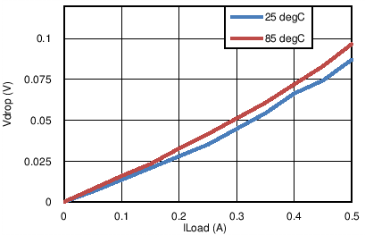
| VGS(Q1) = –1.2 V |
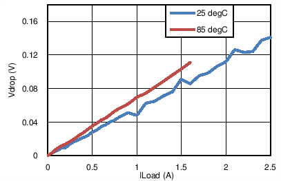
| VGS(Q1) = –2.5 V |
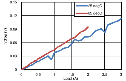
| VGS(Q1) = –4.5 V |
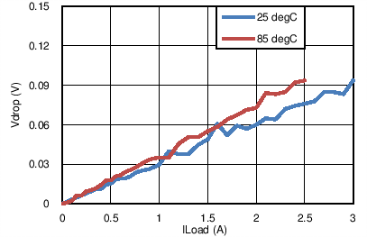
| VGS(Q1) = –7 V |
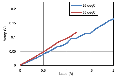
| VGS(Q1) = –1.8 V |
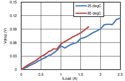
| VGS(Q1) = –3.3 V |
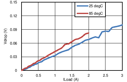
| VGS(Q1) = –5.5 V |
6.6.1 PFET Q1 Minimum Safe Operating Area (SOA)
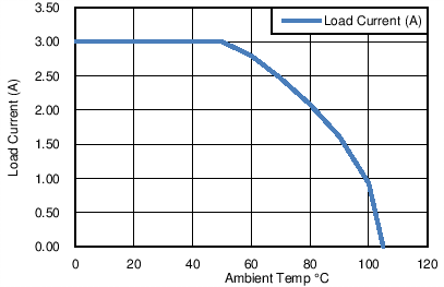
| VGS_Q1 = –4.5 V |
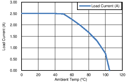
| VGS_Q1 = –2.5 V |
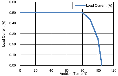
| VGS_Q1 = –1.2 V |
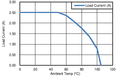
| VGS_Q1 = –3 V |
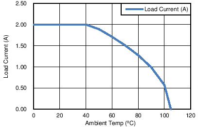
| VGS_Q1 = –1.8 V |