SBVS103D April 2008 – December 2014 TPS3808-EP
PRODUCTION DATA.
- 1 Features
- 2 Applications
- 3 Description
- 4 Revision History
- 5 Pin Configuration and Functions
- 6 Specifications
- 7 Detailed Description
- 8 Application and Implementation
- 9 Power Supply Recommendations
- 10Layout
- 11Device and Documentation Support
- 12Mechanical, Packaging, and Orderable Information
Package Options
Mechanical Data (Package|Pins)
- DBV|6
Thermal pad, mechanical data (Package|Pins)
Orderable Information
1 Features
- Controlled Baseline
- One Assembly Site
- One Test Site
- One Fabrication Site
- Extended Temperature Performance of –55°C to 125°C
- Enhanced Diminishing Manufacturing Sources (DMS) Support
- Enhanced Product-Change Notification
- Qualification Pedigree (1)
- Power-On Reset Generator With Adjustable Delay Time: 1.25 ms to 10 s
- Very Low Quiescent Current: 2.4 μA Typical
- High Threshold Accuracy: 0.5% Typical
- Fixed Threshold Voltages for Standard Voltage Rails From 0.9 V to 5 V and Adjustable Voltage Down to 0.4 V Are Available
- Manual Reset (MR) Input
- Open-Drain RESET Output
- Temperature Range: –55°C to 125°C
- Small SOT-23 Package
2 Applications
- DSP or Microcontroller Applications
- Notebook/Desktop Computers
- PDAs and Hand-Held Products
- Portable and Battery Powered Products
- FPGA and ASIC Applications
3 Description
The TPS3808xxx family of microprocessor supervisory circuits monitors system voltages from 0.4 V to 5.0 V, asserting an open-drain RESET signal when the SENSE voltage drops below a preset threshold or when the manual reset (MR) pin drops to a logic low. The RESET output remains low for the user-adjustable delay time after the SENSE voltage and manual reset (MR) return above the respective thresholds.
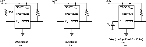
The TPS3808 uses a precision reference to achieve 0.5% threshold accuracy for VIT ≤ 3.3 V. The reset delay time can be set to 20 ms by disconnecting the CT pin, 300 ms by connecting the CT pin to VDD using a resistor, or can be user-adjusted between 1.25 ms and 10 s by connecting the CT pin to an external capacitor. The TPS3808 has a very low typical quiescent current of 2.4 μA, so it is well-suited to battery-powered applications. It is available in a small SOT-23 package, and is fully specified over a temperature range of –55°C to +125°C (TJ).
Device Information(1)
| PART NUMBER | PACKAGE | BODY SIZE (NOM) |
|---|---|---|
| TPS3808-EP | SOT (6) | 2.90 mm x 1.60 mm |
- For all available packages, see the orderable addendum at the end of the datasheet.
Typical Application Circuit