SNVSB03D December   2018  – January 2020 TPS3840

PRODUCTION DATA.  

  1. Features
  2. Applications
  3. Description
    1.     Device Images
      1.      Typical Application Circuit
      2.      TPS3840 Typical Supply Current
  4. Revision History
  5. Device Comparison
  6. Pin Configuration and Functions
    1.     Pin Functions
  7. Specifications
    1. 7.1 Absolute Maximum Ratings
    2. 7.2 ESD Ratings
    3. 7.3 Recommended Operating Conditions
    4. 7.4 Thermal Information
    5. 7.5 Electrical Characteristics
    6. 7.6 Timing Requirements
    7. 7.7 Typical Characteristics
  8. Detailed Description
    1. 8.1 Overview
    2. 8.2 Functional Block Diagram
    3. 8.3 Feature Description
      1. 8.3.1 Input Voltage (VDD)
        1. 8.3.1.1 VDD Hysteresis
        2. 8.3.1.2 VDD Transient Immunity
      2. 8.3.2 User-Programmable Reset Time Delay
      3. 8.3.3 Manual Reset (MR) Input
      4. 8.3.4 Output Logic
        1. 8.3.4.1 RESET Output, Active-Low
        2. 8.3.4.2 RESET Output, Active-High
    4. 8.4 Device Functional Modes
      1. 8.4.1 Normal Operation (VDD > VDD(min))
      2. 8.4.2 VDD Between VPOR and VDD(min)
      3. 8.4.3 Below Power-On-Reset (VDD < VPOR)
  9. Application and Implementation
    1. 9.1 Application Information
    2. 9.2 Typical Application
      1. 9.2.1 Design 1: Dual Rail Monitoring with Power-Up Sequencing
        1. 9.2.1.1 Design Requirements
        2. 9.2.1.2 Detailed Design Procedure
        3. 9.2.1.3 Application Curves
      2. 9.2.2 Design 2: Battery Voltage and Temperature Monitor
        1. 9.2.2.1 Design Requirements
        2. 9.2.2.2 Detailed Design Procedure
      3. 9.2.3 Design 3: Fast Start Undervoltage Supervisor with Level-shifted Input
        1. 9.2.3.1 Design Requirements
        2. 9.2.3.2 Detailed Design Procedure
      4. 9.2.4 Design 4: Voltage Monitor with Back-up Battery Switchover
        1. 9.2.4.1 Design Requirements
        2. 9.2.4.2 Detailed Design Procedure
      5. 9.2.5 Application Curve: TPS3840EVM
  10. 10Power Supply Recommendations
  11. 11Layout
    1. 11.1 Layout Guidelines
    2. 11.2 Layout Example
  12. 12Device and Documentation Support
    1. 12.1 Device Nomenclature
    2. 12.2 Support Resources
    3. 12.3 Trademarks
    4. 12.4 Electrostatic Discharge Caution
    5. 12.5 Glossary
  13. 13Mechanical, Packaging, and Orderable Information

Package Options

Mechanical Data (Package|Pins)
Thermal pad, mechanical data (Package|Pins)
Orderable Information

Design 1: Dual Rail Monitoring with Power-Up Sequencing

A typical application for the TPS3840 is voltage rail monitoring and power-up sequencing as shown in Figure 48. The TPS3840 can be used to monitor any rail above 1.6 V. In this design application, two TPS3840 devices monitor two separate voltage rails and sequences the rails upon power-up. The TPS3840PL30 is used to monitor the 3.3-V main power rail and the TPS3840DL16 is used to monitor the 1.8-V rail provided by the LDO for other system peripherals. The RESET output of the TPS3840PL30 is connected to the ENABLE input of the LDO. A reset event is initiated on either voltage supervisor when the VDD voltage is less than VIT- or when MR is driven low by an external source.
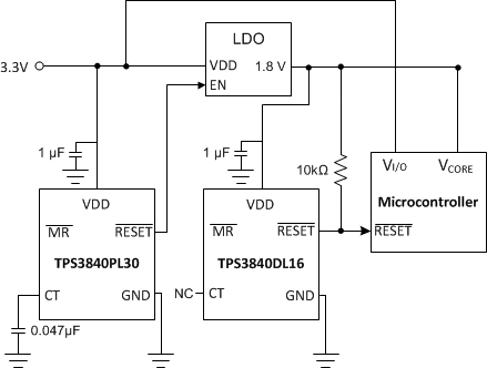
TPS3840 Typical_Application_1rev3.gifFigure 48. TPS3840 Voltage Rail Monitor and Power-Up Sequencer Design Block Diagram