SNVSB03D December 2018 – January 2020 TPS3840
PRODUCTION DATA.
- 1 Features
- 2 Applications
- 3 Description
- 4 Revision History
- 5 Device Comparison
- 6 Pin Configuration and Functions
- 7 Specifications
- 8 Detailed Description
-
9 Application and Implementation
- 9.1 Application Information
- 9.2 Typical Application
- 10Power Supply Recommendations
- 11Layout
- 12Device and Documentation Support
- 13Mechanical, Packaging, and Orderable Information
Package Options
Mechanical Data (Package|Pins)
- DBV|5
Thermal pad, mechanical data (Package|Pins)
Orderable Information
7.7 Typical Characteristics
Typical characteristics show the typical performance of the TPS3840 device. Test conditions are TJ = 25°C, VDD = 3.3 V, Rpull-up = 100 kΩ, CLoad = 50 pF, unless otherwise noted.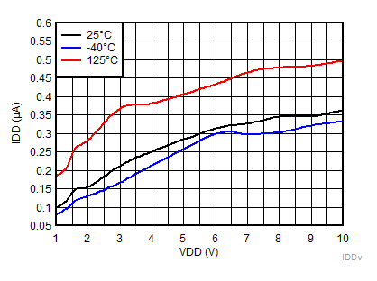 Figure 7. Supply Current vs Supply Voltage for TPS3840DL49
 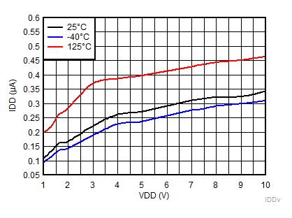 Figure 9. Supply Current vs Supply Voltage for TPS3840PH49
 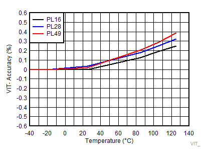 Figure 11. Negative-going Input Threshold Accuracy over Temperature for TPS3840PLXX
 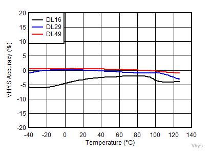 Figure 13. Input Threshold VIT- Hysteresis Accuracy for TPS3840DLXX
 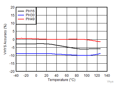 Figure 15. Input Threshold VIT- Hysteresis Accuracy for TPS3840PHXX
 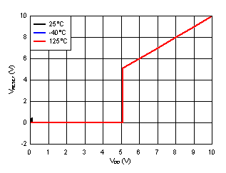 Figure 17. Output Voltage vs Input Voltage for TPS3840PL49
 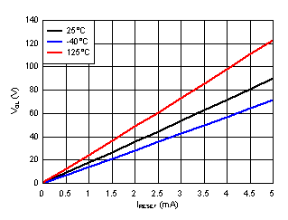 Figure 19. Low Level Output Voltage vs IRESET for TPS3840DL49
 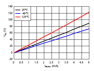 Figure 21. Low Level Output Voltage vs IRESET for TPS3840PL49
 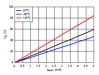 Figure 23. Low Level Output Voltage vs IRESET for TPS3840PH49
 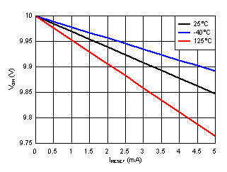 Figure 25. High Level Output Voltage vs IRESET for TPS3840PL49
 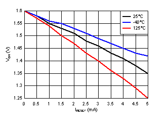 Figure 27. High Level Output Voltage vs IRESET for TPS3840PH49
 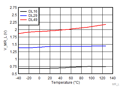 Figure 29. Manual Reset Logic Low Voltage Threshold over Temperature for TPS3840DLXX
 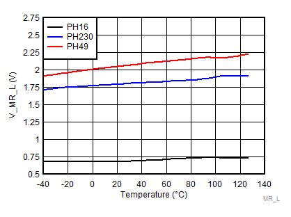 Figure 31. Manual Reset Logic Low Voltage Threshold over Temperature for TPS3840PHXX
 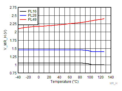 Figure 33. Manual Reset Logic High Voltage Threshold over Temperature for TPS3840PLXX
 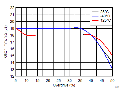 Figure 35. Glitch Immunity on VIT- vs Overdrive (Data Taken with TPS3840PL28)
 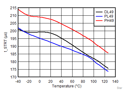 Figure 37. Startup Delay over Temperature
 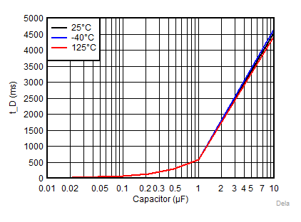 Figure 39. Reset Time Delay vs Capacitor Value (Data Taken with TPS3840PL16)
 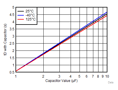 Figure 41. Reset Time Delay vs Large Capacitor Values (Data Taken with TPS3840PL16)
 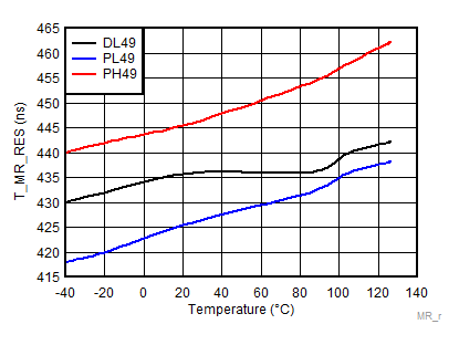 Figure 43. Propagation Time Delay from MR Asserted to Reset over Temperature
 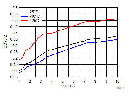 Figure 8. Supply Current vs Supply Voltage for TPS3840PL49
 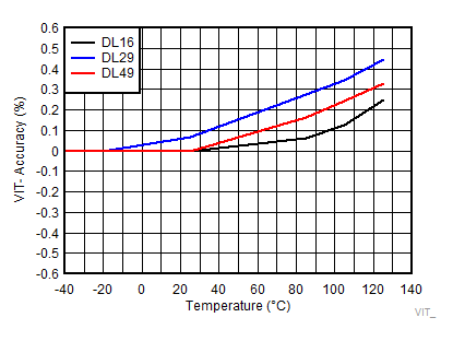 Figure 10. Negative-going Input Threshold Accuracy over Temperature for TPS3840DLXX
 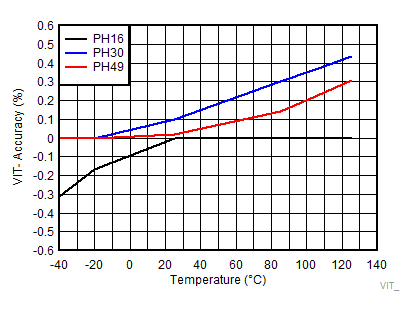 Figure 12. Negative-going Input Threshold Accuracy over Temperature for TPS3840PHXX
 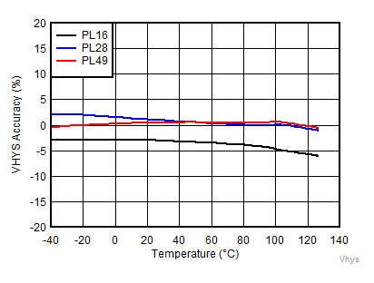 Figure 14. Input Threshold VIT- Hysteresis Accuracy for TPS3840PLXX
 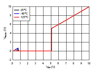 Figure 16. Output Voltage vs Input Voltage for TPS3840DL49
 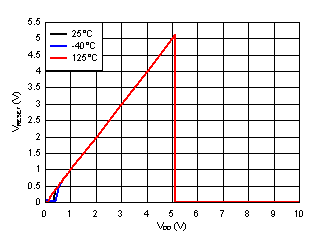 Figure 18. Output Voltage vs Input Voltage for TPS3840PH49
 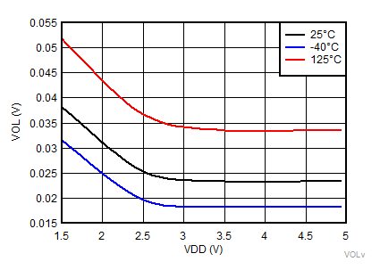 Figure 20. Low Level Output Voltage vs VDD for TPS3840DL49
 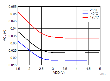 Figure 22. Low Level Output Voltage vs VDD for TPS3840PL49
 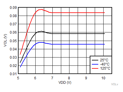 Figure 24. Low Level Output Voltage vs VDD for TPS3840PH49
 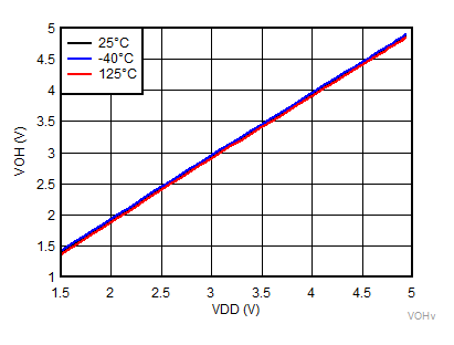 Figure 26. High Level Output Voltage over Temperature for TPS3840PL49
  Figure 28. High Level Output Voltage over Temperature for TPS3840PH49
 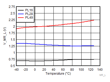 Figure 30. Manual Reset Logic Low Voltage Threshold over Temperature for TPS3840PLXX
 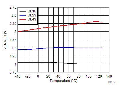 Figure 32. Manual Reset Logic High Voltage Threshold over Temperature for TPS3840DLXX
 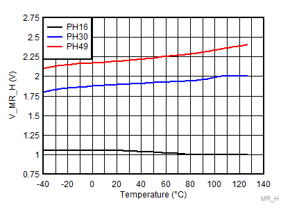 Figure 34. Manual Reset Logic High Voltage Threshold over Temperature for TPS3840PHXX
 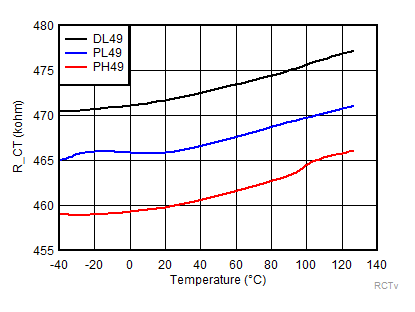 Figure 36. CT Pin Internal Resistance over Temperature
 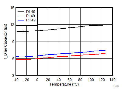 Figure 38. Reset Time Delay with No Capacitor over Temperature
 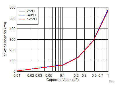 Figure 40. Reset Time Delay vs Small Capacitor Values (Data Taken with TPS3840PL16)
 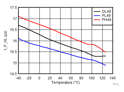 Figure 42. Propagation Detect Time Delay for VDD Falling Below VIT- (High-to-Low) over Temperature
 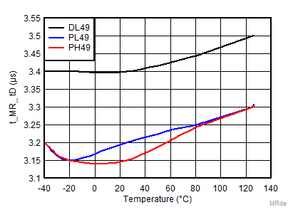 Figure 44. Propagation Time Delay from MR Release to Deasserted Reset over Temperature