SLVSA75A July 2010 – August 2015 TPS386596
PRODUCTION DATA.
- 1 Features
- 2 Applications
- 3 Description
- 4 Revision History
- 5 Pin Configuration and Functions
- 6 Specifications
- 7 Parameter Measurement Information
- 8 Detailed Description
- 9 Application and Implementation
- 10Power Supply Recommendations
- 11Layout
- 12Device and Documentation Support
- 13Mechanical, Packaging, and Orderable Information
Package Options
Mechanical Data (Package|Pins)
- DGK|8
Thermal pad, mechanical data (Package|Pins)
- DGK|8
Orderable Information
11 Layout
11.1 Layout Guidelines
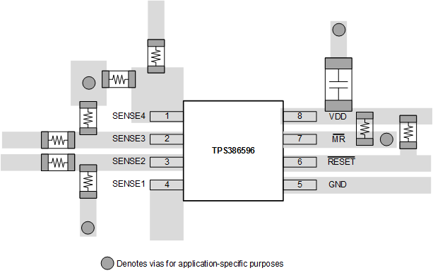
Follow these guidelines to lay out the printed-circuit-board (PCB) that is used for the TPS386596.
- Avoid long traces from the SENSE pin to the resistor divider. Instead, run the long traces from the RSnH to VMON(n).
- Place the VDD decoupling capacitor (CVDD) close to the device.
- Avoid using long traces for the VDD supply node. The VDD capacitor (CVDD), along with parasitic inductance from the supply to the capacitor, can form an LC tank and create ringing with peak voltages above the maximum VDD voltage.
11.2 Layout Example
 Figure 20. Example Layout (DGK Package)