SLUS660I September 2005 – January 2015 TPS40140
PRODUCTION DATA.
- 1 Features
- 2 Applications
- 3 Description
- 4 Revision History
- 5 Device Comparison Table
- 6 Pin Configuration and Functions
- 7 Specifications
- 8 Detailed Description
-
9 Application and Implementation
- 9.1
Application Information
- 9.1.1 Synchronizing a Single Controller to an External Clock
- 9.1.2 Split Input Voltage Operation
- 9.1.3 Configuring Single and Multiple ICs
- 9.1.4 Digital Clock Synchronization
- 9.1.5 Typical Start-Up Sequence
- 9.1.6 Track (Soft-Start Without PreBiased Output)
- 9.1.7 Soft-Start With PreBiased Outputs
- 9.1.8 Track Function in Configuring a Slave Channel
- 9.1.9 Differential Amplifier, U9
- 9.1.10 Setting the Output Voltage
- 9.1.11 Programmable Input UVLO Protection
- 9.1.12 CLKFLT, CLKIO Pin Fault
- 9.1.13 PHSEL Pin Fault
- 9.1.14 Overtemperature
- 9.1.15 Fault Masking Operation
- 9.1.16 Setting the Switching Frequency
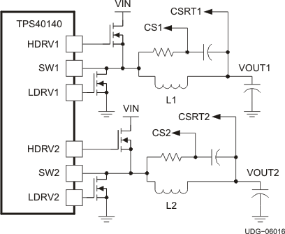
- 9.1.17 Current Sense
- 9.1.18 Current Sensing and Balancing
- 9.1.19 Overcurrent Detection and Hiccup Mode
- 9.1.20 Calculating Overcurrent Protection Level
- 9.1.21 Design Examples Information
- 9.2
Typical Application
- 9.2.1
Application 1: Dual-Output Configuration from 12 to 3.3 V and 1.5 V DC-DC Converter Using a TPS40140
- 9.2.1.1 Design Requirements
- 9.2.1.2
Detailed Design Procedure
- 9.2.1.2.1 Step 1: Inductor Selection
- 9.2.1.2.2 Step 2: Output Capacitor Selection
- 9.2.1.2.3 Step 3: Input Capacitor Selection
- 9.2.1.2.4 Step 4: MOSFET Selection
- 9.2.1.2.5
Step 5: Peripheral Component Design
- 9.2.1.2.5.1 Switching Frequency Setting (RT Pin 5)
- 9.2.1.2.5.2 Output Voltage Setting (FB1 Pin 36)
- 9.2.1.2.5.3 Current Sensing Network Design (CS1 Pin 31 and CSRT1 Pin 32)
- 9.2.1.2.5.4 Overcurrent Protection (ILIM1 Pin 34)
- 9.2.1.2.5.5 VREG (Pin 21)
- 9.2.1.2.5.6 BP5 (Pin 8)
- 9.2.1.2.5.7 PHSEL (Pin 4)
- 9.2.1.2.5.8 VSHARE (Pin 6)
- 9.2.1.2.5.9 PGOOD1 (Pin 30)
- 9.2.1.2.5.10 UVLO_CE1 (Pin 29)
- 9.2.1.2.5.11 Clkio (Pin 28)
- 9.2.1.2.5.12 BOOT1 and SW1 (Pin 27 and 25)
- 9.2.1.2.5.13 TRK1 (Pin 33)
- 9.2.1.2.5.14 DIFFO, VOUT, and GSNS (Pin 1, Pin 2, and Pin 3)
- 9.2.1.2.6 Feedback Compensator Design (COMP1 Pin 35)
- 9.2.1.3 Application Curves
- 9.2.2
Application 2: Two-Phase Single Output Configuration from 12 to 1.5 V DC-DC Converter Using a TPS40140
- 9.2.2.1 Design Requirements
- 9.2.2.2
Detailed Design Procedure
- 9.2.2.2.1 Step 1: Output Capacitor Selection
- 9.2.2.2.2 Step 2: Input Capacitor Selection
- 9.2.2.2.3
Step 3: Peripheral Component Design
- 9.2.2.2.3.1 Switching Frequency Setting (Rt Pin 5)
- 9.2.2.2.3.2 COMP1 and COMP2 (Pin 35 and Pin 10)
- 9.2.2.2.3.3 TRK1 and TRK2 (Pin 33 and Pin 12)
- 9.2.2.2.3.4 ILIM1 and ILIM2 (Pin 34 and Pin 11)
- 9.2.2.2.3.5 FB1 and FB2 (Pin 36 and Pin 9)
- 9.2.2.2.3.6 PHSEL (Pin 4)
- 9.2.2.2.3.7 PGOOD1 and PGOOD2 (Pin 30 and Pin 15)
- 9.2.2.2.3.8 CLKIO (Pin 28)
- 9.2.2.2.3.9 DIFFO, VOUT, and GSNS (Pin 1, Pin 2, and Pin 3)
- 9.2.3 Application Curves
- 9.2.1
Application 1: Dual-Output Configuration from 12 to 3.3 V and 1.5 V DC-DC Converter Using a TPS40140
- 9.3
System Example
- 9.3.1
Four-Phase Single Output Configuration from 12 to 1.8 V DC-DC Converter Using Two TPS40140
- 9.3.1.1 Step 1: Output Capacitor Selection
- 9.3.1.2 Step 2: Input Capacitor Selection
- 9.3.1.3
Step 3: Peripheral Component Design
- 9.3.1.3.1
Master Module
- 9.3.1.3.1.1 Rt (Pin 5)
- 9.3.1.3.1.2 COMP1 and COMP2 (Pin 35 and Pin 10)
- 9.3.1.3.1.3 TRK1 and TRK2 (Pin 33 and Pin 12)
- 9.3.1.3.1.4 ILIM1 and ILIM2 (Pin 34 and Pin 11)
- 9.3.1.3.1.5 FB1 and FB2 (Pin 36 and Pin 9)
- 9.3.1.3.1.6 PHSEL (Pin 4)
- 9.3.1.3.1.7 PGOOD1 and PGOOD2 (Pin 30 and Pin 15)
- 9.3.1.3.1.8 CLKIO (Pin 28)
- 9.3.1.3.2
Slave Module:
- 9.3.1.3.2.1 RT (Pin 5)
- 9.3.1.3.2.2 COMP1 and COMP2 (Pin 35 and Pin 10)
- 9.3.1.3.2.3 TRK1 and TRK2 (Pin 33 and Pin 12)
- 9.3.1.3.2.4 ILIM1 and ILIM2 ( Pin 34 and Pin 11)
- 9.3.1.3.2.5 FB1 and FB2 (Pin 36 and Pin 9)
- 9.3.1.3.2.6 PHSEL (Pin 4)
- 9.3.1.3.2.7 PGOOD1 and PGOOD2 (Pin 30 and Pin 15)
- 9.3.1.3.2.8 CLKIO (Pin 28)
- 9.3.1.3.1
Master Module
- 9.3.1
Four-Phase Single Output Configuration from 12 to 1.8 V DC-DC Converter Using Two TPS40140
- 9.1
Application Information
- 10Power Supply Recommendations
- 11Layout
- 12Device and Documentation Support
- 13Mechanical, Packaging, and Orderable Information
Package Options
Mechanical Data (Package|Pins)
- RHH|36
Thermal pad, mechanical data (Package|Pins)
- RHH|36
Orderable Information
1 Features
- VDD from 4.5 to 15 V, With Internal 5-V Regulator
- VOUT from 0.7 V to 5.8 V
- Converts from 15-V Input to 0.7-V Output at
1 MHz - Dual-Output or 2-Phase Interleaved Operation, Stackable to 16 Phases
- Supports Prebiased Outputs
- 0.5% Internally Trimmed 0.7-V Reference
- 10-μA Shutdown Current
- Current Mode Control With Forced Current Sharing (1)
- 1- to 40-V Power Stage Operation Range
- Power Sharing From Different Input Voltage Rails, (for Example, Master From 5 V, Slave From 12 V)
- True Remote Sensing Differential Amplifier
- Programmable Input Undervoltage Lockout (UVLO)
- Resistive or Inductor DCR Current Sensing
- Provide a 6-Bit Digitally Controlled Output When Used With TPS40120
- 36-Pin VQFN Package
Programmable Switching Frequency up to
1 MHz/Phase
2 Applications
- Graphic Cards
- Internet Servers
- Networking Equipment
- Telecommunications Equipment
- DC Power Distributed Systems
3 Description
The TPS40140 is a multifunctional synchronous buck controller that can be configured to provide either a single-output 2-phase power supply or a power supply that supports two independent outputs. Several TPS40140 controllers can be stacked up to a 16-phase single output power supply. Alternatively, several controllers providing multiple independent outputs can be synchronized in an interleaving pattern for improved input ripple current.
The TPS40140 can convert from a 15-V input to a 0.7-V output at 1 MHz.
Each phase operates at a switching frequency of up to 1 MHz. The two phases in one device operate 180° out-of-phase. In a multiple-device stackable configuration, the phase shift of the slaves, relative to a master, is programmable.
Device Information(1)
| PART NUMBER | PACKAGE | BODY SIZE (NOM) |
|---|---|---|
| TPS40140 | VQFN (36) | 6.00 mm × 6.00 mm |
- For all available packages, see the orderable addendum at the end of the data sheet.
Simplified Schematic