SLUS660I September 2005 – January 2015 TPS40140
PRODUCTION DATA.
- 1 Features
- 2 Applications
- 3 Description
- 4 Revision History
- 5 Device Comparison Table
- 6 Pin Configuration and Functions
- 7 Specifications
- 8 Detailed Description
-
9 Application and Implementation
- 9.1
Application Information
- 9.1.1 Synchronizing a Single Controller to an External Clock
- 9.1.2 Split Input Voltage Operation
- 9.1.3 Configuring Single and Multiple ICs
- 9.1.4 Digital Clock Synchronization
- 9.1.5 Typical Start-Up Sequence
- 9.1.6 Track (Soft-Start Without PreBiased Output)
- 9.1.7 Soft-Start With PreBiased Outputs
- 9.1.8 Track Function in Configuring a Slave Channel
- 9.1.9 Differential Amplifier, U9
- 9.1.10 Setting the Output Voltage
- 9.1.11 Programmable Input UVLO Protection
- 9.1.12 CLKFLT, CLKIO Pin Fault
- 9.1.13 PHSEL Pin Fault
- 9.1.14 Overtemperature
- 9.1.15 Fault Masking Operation
- 9.1.16 Setting the Switching Frequency
- 9.1.17 Current Sense
- 9.1.18 Current Sensing and Balancing
- 9.1.19 Overcurrent Detection and Hiccup Mode
- 9.1.20 Calculating Overcurrent Protection Level
- 9.1.21 Design Examples Information
- 9.2
Typical Application
- 9.2.1
Application 1: Dual-Output Configuration from 12 to 3.3 V and 1.5 V DC-DC Converter Using a TPS40140
- 9.2.1.1 Design Requirements
- 9.2.1.2
Detailed Design Procedure
- 9.2.1.2.1 Step 1: Inductor Selection
- 9.2.1.2.2 Step 2: Output Capacitor Selection
- 9.2.1.2.3 Step 3: Input Capacitor Selection
- 9.2.1.2.4 Step 4: MOSFET Selection
- 9.2.1.2.5
Step 5: Peripheral Component Design
- 9.2.1.2.5.1 Switching Frequency Setting (RT Pin 5)
- 9.2.1.2.5.2 Output Voltage Setting (FB1 Pin 36)
- 9.2.1.2.5.3 Current Sensing Network Design (CS1 Pin 31 and CSRT1 Pin 32)
- 9.2.1.2.5.4 Overcurrent Protection (ILIM1 Pin 34)
- 9.2.1.2.5.5 VREG (Pin 21)
- 9.2.1.2.5.6 BP5 (Pin 8)
- 9.2.1.2.5.7 PHSEL (Pin 4)
- 9.2.1.2.5.8 VSHARE (Pin 6)
- 9.2.1.2.5.9 PGOOD1 (Pin 30)
- 9.2.1.2.5.10 UVLO_CE1 (Pin 29)
- 9.2.1.2.5.11 Clkio (Pin 28)
- 9.2.1.2.5.12 BOOT1 and SW1 (Pin 27 and 25)
- 9.2.1.2.5.13 TRK1 (Pin 33)
- 9.2.1.2.5.14 DIFFO, VOUT, and GSNS (Pin 1, Pin 2, and Pin 3)
- 9.2.1.2.6 Feedback Compensator Design (COMP1 Pin 35)
- 9.2.1.3 Application Curves
- 9.2.2
Application 2: Two-Phase Single Output Configuration from 12 to 1.5 V DC-DC Converter Using a TPS40140
- 9.2.2.1 Design Requirements
- 9.2.2.2
Detailed Design Procedure
- 9.2.2.2.1 Step 1: Output Capacitor Selection
- 9.2.2.2.2 Step 2: Input Capacitor Selection
- 9.2.2.2.3
Step 3: Peripheral Component Design
- 9.2.2.2.3.1 Switching Frequency Setting (Rt Pin 5)
- 9.2.2.2.3.2 COMP1 and COMP2 (Pin 35 and Pin 10)
- 9.2.2.2.3.3 TRK1 and TRK2 (Pin 33 and Pin 12)
- 9.2.2.2.3.4 ILIM1 and ILIM2 (Pin 34 and Pin 11)
- 9.2.2.2.3.5 FB1 and FB2 (Pin 36 and Pin 9)
- 9.2.2.2.3.6 PHSEL (Pin 4)
- 9.2.2.2.3.7 PGOOD1 and PGOOD2 (Pin 30 and Pin 15)
- 9.2.2.2.3.8 CLKIO (Pin 28)
- 9.2.2.2.3.9 DIFFO, VOUT, and GSNS (Pin 1, Pin 2, and Pin 3)
- 9.2.3 Application Curves
- 9.2.1
Application 1: Dual-Output Configuration from 12 to 3.3 V and 1.5 V DC-DC Converter Using a TPS40140
- 9.3
System Example
- 9.3.1
Four-Phase Single Output Configuration from 12 to 1.8 V DC-DC Converter Using Two TPS40140
- 9.3.1.1 Step 1: Output Capacitor Selection
- 9.3.1.2 Step 2: Input Capacitor Selection
- 9.3.1.3
Step 3: Peripheral Component Design
- 9.3.1.3.1
Master Module
- 9.3.1.3.1.1 Rt (Pin 5)
- 9.3.1.3.1.2 COMP1 and COMP2 (Pin 35 and Pin 10)
- 9.3.1.3.1.3 TRK1 and TRK2 (Pin 33 and Pin 12)
- 9.3.1.3.1.4 ILIM1 and ILIM2 (Pin 34 and Pin 11)
- 9.3.1.3.1.5 FB1 and FB2 (Pin 36 and Pin 9)
- 9.3.1.3.1.6 PHSEL (Pin 4)
- 9.3.1.3.1.7 PGOOD1 and PGOOD2 (Pin 30 and Pin 15)
- 9.3.1.3.1.8 CLKIO (Pin 28)
- 9.3.1.3.2
Slave Module:
- 9.3.1.3.2.1 RT (Pin 5)
- 9.3.1.3.2.2 COMP1 and COMP2 (Pin 35 and Pin 10)
- 9.3.1.3.2.3 TRK1 and TRK2 (Pin 33 and Pin 12)
- 9.3.1.3.2.4 ILIM1 and ILIM2 ( Pin 34 and Pin 11)
- 9.3.1.3.2.5 FB1 and FB2 (Pin 36 and Pin 9)
- 9.3.1.3.2.6 PHSEL (Pin 4)
- 9.3.1.3.2.7 PGOOD1 and PGOOD2 (Pin 30 and Pin 15)
- 9.3.1.3.2.8 CLKIO (Pin 28)
- 9.3.1.3.1
Master Module
- 9.3.1
Four-Phase Single Output Configuration from 12 to 1.8 V DC-DC Converter Using Two TPS40140
- 9.1
Application Information
- 10Power Supply Recommendations
- 11Layout
- 12Device and Documentation Support
- 13Mechanical, Packaging, and Orderable Information
Package Options
Mechanical Data (Package|Pins)
- RHH|36
Thermal pad, mechanical data (Package|Pins)
- RHH|36
Orderable Information
7 Specifications
7.1 Absolute Maximum Ratings
over operating free-air temperature range (unless otherwise noted)7.2 ESD Ratings
| VALUE | UNIT | |||
|---|---|---|---|---|
| V(ESD) | Electrostatic discharge | Human body model (HBM), per ANSI/ESDA/JEDEC JS-001(1) | 3000 | V |
| Charged-device model (CDM), per JEDEC specification JESD22-C101(2) | 1500 | |||
(1) JEDEC document JEP155 states that 500-V HBM allows safe manufacturing with a standard ESD control process.
(2) JEDEC document JEP157 states that 250-V CDM allows safe manufacturing with a standard ESD control process.
7.3 Recommended Operating Conditions
over operating free-air temperature range (unless otherwise noted)| MIN | NOM | MAX | UNIT | |||
|---|---|---|---|---|---|---|
| Input voltage | VDD, UVLO ≤ VDD | –0.3 | 15 | V | ||
| SW1, SW2 | –1 | 40 | ||||
| BOOT1, BOOT2, HDRV1, HDRV2 | VSW + 5.5 | |||||
| All other pins | –0.3 | 5.5 | ||||
| Maximum output current | RT | 25 | µA | |||
| Operating free-air temperature | –40 | 85 | °C | |||
7.4 Thermal Information
| THERMAL METRIC(1) | TPS40140 | UNIT | |
|---|---|---|---|
| RHH (VQFN) |
|||
| 36 PINS | |||
| RθJA | Junction-to-ambient thermal resistance | 30.8 | °C/W |
| RθJC(top) | Junction-to-case (top) thermal resistance | 18.4 | |
| RθJB | Junction-to-board thermal resistance | 5.9 | |
| ψJT | Junction-to-top characterization parameter | 0.2 | |
| ψJB | Junction-to-board characterization parameter | 5.9 | |
| RθJC(bot) | Junction-to-case (bottom) thermal resistance | 0.7 | |
(1) For more information about traditional and new thermal metrics, see the IC Package Thermal Metrics application report, SPRA953.
7.5 Electrical Characteristics
–40°C ≤ TJ ≤ 85°C, (unless otherwise noted), VVDD = 7 V, VBP5 = 5 V, UVLO_CE1, UCLO_CE2: 10 kΩ, Pullup to BP5,ƒSW = 300 kHz, unless otherwise noted
| PARAMETER | TEST CONDITIONS | MIN | TYP | MAX | UNIT | |
|---|---|---|---|---|---|---|
| VDD INPUT SUPPLY | ||||||
| Operating voltage range | 4.5 | 12 | 15 | V | ||
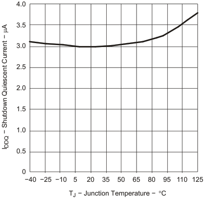
| Shutdown current | UVLO_CE1 = UVLO_CE2 = GND | 1 | 10 | µA | ||
| BP5 INPUT SUPPLY | ||||||
| Operating voltage range | 4.5 | 5.0 | 5.5 | V | ||
| BP5 operating current | 2 | 3 | 5 | mA | ||
| Rising BP5 turnon | 4.0 | 4.25 | 4.45 | V | ||
| BP5 turnoff hysteresis | 100 | 220 | 400 | mV | ||
| Standby mode current(1) | UVLO_CEx = 1.7 V | 2.8 | mA | |||
| VREG | ||||||
| 7 V < VDD < 15 V | 4.5 | 5.1 | 5.5 | V | ||
| Output current | 0 | 100 | mA | |||
| OSCILLATOR, RT | ||||||
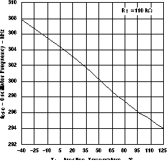
| Phase frequency accuracy | RRT= 110 kΩ | 300 | kHz | |||
| Phase frequency set range | 150 | 1000 | kHz | |||
| RT(1) | 25 kΩ ≤ RRT ≤ 500 kΩ | 0.7 | V | |||
| UNDERVOLTAGE LOCKOUT (UVLO_CE1, UVLO_CE2) | ||||||
| Enable threshold, standby mode | Internal 5VREG regulator enabled | 0.5 | 1.0 | 1.5 | V | |
| UVLO threshold | PWM Switching enabled | 1.9 | 2 | 2.1 | V | |
| UVLO hysteresis | At the UVLO_CEx pin | 40 | mV | |||
| UVLO_CE1, UVLO_CE2 bias current(1) | 1 | μA | ||||
| PWM | ||||||
| DMAX | Maximum duty cycle per channel(1) | 2-phase, 4-phase, 8-phase, or 16-phase | 87.5% | |||
| 3-phase, 6-phase, or 12-phase | 83.3% | |||||
| tON(min) | Minimum controllable pulse width | 70 | ns | |||
| PWM COMPARATOR | ||||||
| Input offset voltage | –3 | 3 | mV | |||
| VSHARE | ||||||
| IVSHR = 0 | 1.785 | 1.8 | 1.815 | V | ||
| See(1) | –30 μA < iVSHR < 50 μA | 1.785 | 1.8 | 1.815 | V | |
| ERROR AMPLIFIER CH1, ERROR AMPLIFIER CH2 | ||||||
| Input common mode range(1) | 0 | 0.7 | 2.0 | V | ||
| Input bias current(1) | VFB = 0.7 V | 10 | nA | |||
| FBx voltage(1) | 0.6965 | 0.700 | 0.7035 | V | ||
| Output source current | VCOMP = 1.1 V, VFB = 0.6 V | 1 | 2 | mA | ||
| Output sink current | VCOMP = 1.1 V, VFB = BP5 | 1 | 2 | mA | ||
| BW(1) | 8 | 12 | MHz | |||
| Open loop gain(1) | 60 | 90 | dB | |||
| VOLTAGE TRACKING (TRK1, TRK2) | ||||||
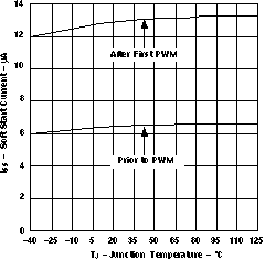
| SS source current | After EN, before PWM and during hiccup mode | 5 | 6.0 | 7.3 | µA | |
| After first PWM pulse | 10 | 12.5 | 15 | |||
| Fault enable threshold(1) | 1.4 | V | ||||
| Internal clamp voltage(1) | 2.4 | V | ||||
| SS sink resistance(1) | Pulldown resistance | 1 | kΩ | |||
| CURRENT SENSE AMPLIFIERS (CS1, CS2) | ||||||
| Differential input voltage | –60 | 60 | mV | |||
| Input offset voltage | CS1, CS2, trimmed | –2.0 | 0 | 2.0 | mV | |
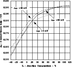
| Ac | Gain transfer to PWM COMP | 5 mV < VCS < 60 mV, VCSRT = 1.5 V | 12 | 13 | 14 | V/V |
| Input common mode(1) | 0 | 5.8 | V | |||
| CSA | Input bias current | 100 | nA | |||
| DIFFERENTIAL AMPLIFIER (DIFFO) | ||||||
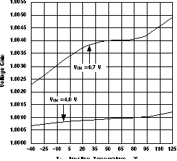
| Gain | 1.0 V < VOUT < 5.8 V | 0.997 | 1 | 1.003 | V/V | |
| Input common mode range(1) | 0 | 5.8 | V | |||
| Output source current(1) | VOUT – VVGSNS = 2 V, VDIFFO > 1.98 V, VDD-VOUT > 2 V |
2 | mA | |||
| Output source current(1) | VOUT – VVGSNS = 2 V, VDIFFO > 2.02 V VDD – VOUT = 1 V | 1 | ||||
| Output sink current(1) | VOUT – VVGSNS = 2 V, VDIFFO > 2.02 V |
2 | ||||
| Unity gain bandwidth(1) | 5 | 8 | MHz | |||
| Input Impedance, non inverting(1) | VOUT to GND | 60 | kΩ | |||
| Input Impedance, inverting(1) | GSNS to DIFFO | 60 | ||||
| GATE DRIVERS | ||||||
| HDRV1, HDRV2 source on-resistance | VBOOT1, VBOOT2 = 5 V, VSW1 = VSW2 = 0 V, Sourcing 100 mA |
1 | 2 | 3 | Ω | |
| HDRV1, HDRV2 sink on-resistance | VVREG = 5 V, VSW1 = VSW2 = 0 V, Sinking 100 mA |
0.5 | 1.2 | 2 | ||
| LDRV1, LDRV2 source on-resistance | VVREG = 5 V, VSW1 = VSW2 = 0 V, Sourcing 100 mA |
1 | 2 | 3 | ||
| LDRV1, LDRV2 sink on-resistance | VVREG = 5 V, VSW1 = VSW2 = 0 V, Sinking 100 mA |
0.3 | 0.65 | 1 | ||
| tRISE | HDRVx rise time(1) | CLOAD= 3.3 nF | 25 | 75 | ns | |
| tFALL | HDRVx fall time(1) | CLOAD= 3.3 nF | 25 | 75 | ||
| tRISE | LDRVx rise time(1) | CLOAD= 3.3 nF | 25 | 75 | ||
| tFALL | LDRVx fall time(1) | CLOAD= 3.3 nF | 20 | 60 | ||
| Minimum controllable on-time | CLOAD= 3.3 nF | 50 | ||||
| OUTPUT UNDERVOLTAGE FAULT | ||||||
| VFB relative to VREF | –19% | –16.5% | –14% | |||
| Undervoltage delay(1) | 3 | µs | ||||
| CURRENT LIMIT | ||||||
| IILIM | Output current | 18.8 | 20 | 21.2 | µA | |
| POWER GOOD | ||||||
| PGOOD transition low threshold | VFB rising relative to VREF | 10% | 12.5% | 15% | ||
| PGOOD transition low threshold | VFB falling relative to VREF | –15% | –12.5% | –10% | ||
| PGOOD trip hysteresis | 2% | 5% | ||||
| PGOOD delay(1) | 10 | µs | ||||
| Low level output voltage, VOL | IPGOOD = 4 mA | 0.35 | 0.4 | V | ||
| PGOOD bias current | VPGOOD= 5.0 V | –2 | 1 | 2 | µA | |
| RAMP | ||||||
| Ramp amplitude(1) | 0.421 | 0.5 | 0.526 | V | ||
| VIN BALANCE | ||||||
| VIN balance gain, AVB | 0.23 | 0.25 | 0.27 | V/V | ||
| THERMAL SHUTDOWN | ||||||
| Shutdown temperature(1) | 155 | °C | ||||
| Hysteresis(1) | 30 | |||||
| DIGITAL CLOCK SIGNAL (CLKIO) | ||||||
| Pullup resistance(1) | IOH = 5 mA | 27 | Ω | |||
| Pulldown resistance(1) | IOL = 10 mA | 27 | Ω | |||
| Output leakage(1) | Tri-state | 1 | µA | |||
(1) Specified by design. Not production tested.
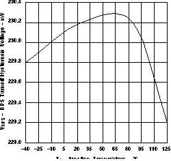
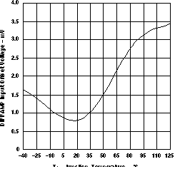
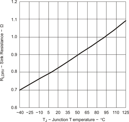
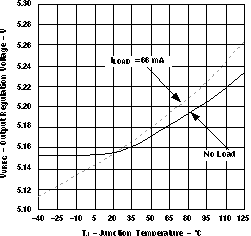
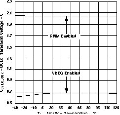
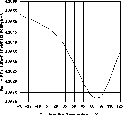
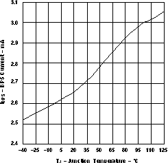
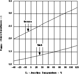
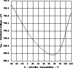
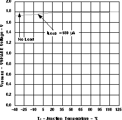
7.6 Typical Characteristics