SLUSBO6C JANUARY 2014 – October 2018 TPS40425
PRODUCTION DATA.
- 1 Features
- 2 Applications
- 3 Description
- 4 Revision History
- 5 Pin Configuration and Functions
- 6 Specifications
-
7 Detailed Description
- 7.1 Overview
- 7.2 Functional Block Diagram
- 7.3
Feature Description
- 7.3.1 Asynchronous Pulse Injection (API)
- 7.3.2 Adaptive Voltage Scaling (AVS)
- 7.3.3 Switching Frequency and Synchronization
- 7.3.4 Voltage Reference
- 7.3.5 Output Voltage and Remote Sensing Amplifier
- 7.3.6 Current Sensing and Temperature Sensing Modes
- 7.3.7 Current Sensing
- 7.3.8 Temperature Sensing
- 7.3.9 Current Sharing
- 7.3.10 Linear Regulators
- 7.3.11 Power Sequence Between TPS40425 Device and Power Stage
- 7.3.12 PWM Signal
- 7.3.13 Startup and Shutdown
- 7.3.14 Pre-Biased Output Start-up
- 7.3.15 PGOOD Indication
- 7.3.16 Overcurrent Protection
- 7.3.17 Overvoltage/Undervoltage Protection
- 7.3.18 Overtemperature Fault Protection
- 7.3.19 Input Undervoltage Lockout (UVLO)
- 7.3.20 Fault Communication
- 7.3.21 Fault Protection Summary
- 7.4 Device Functional Modes
- 7.5 Programming
- 7.6 Register Maps
- 7.7
Supported PMBus Commands
- 7.7.1 PAGE (00h)
- 7.7.2 OPERATION (01h)
- 7.7.3 ON_OFF_CONFIG (02h)
- 7.7.4 CLEAR_FAULTS (03h)
- 7.7.5 WRITE_PROTECT (10h)
- 7.7.6 STORE_USER_ALL (15h)
- 7.7.7 RESTORE_USER_ALL (16h)
- 7.7.8 CAPABILITY (19h)
- 7.7.9 VOUT_MODE (20h)
- 7.7.10 VIN_ON (35h)
- 7.7.11 VIN_OFF (36h)
- 7.7.12 IOUT_CAL_GAIN (38h)
- 7.7.13 IOUT_CAL_OFFSET (39h)
- 7.7.14 IOUT_OC_FAULT_LIMIT (46h)
- 7.7.15 IOUT_OC_FAULT_RESPONSE (47h)
- 7.7.16 IOUT_OC_WARN_LIMIT (4Ah)
- 7.7.17 OT_FAULT_LIMIT (4Fh)
- 7.7.18 OT_WARN_LIMIT (51h)
- 7.7.19 TON_RISE (61h)
- 7.7.20 STATUS_BYTE (78h)
- 7.7.21 STATUS_WORD (79h)
- 7.7.22 STATUS_VOUT (7Ah)
- 7.7.23 STATUS_IOUT (7Bh)
- 7.7.24 STATUS_TEMPERATURE (7Dh)
- 7.7.25 STATUS_CML (7Eh)
- 7.7.26 STATUS_MFR_SPECIFIC (80h)
- 7.7.27 READ_VOUT (8Bh)
- 7.7.28 READ_IOUT (8Ch)
- 7.7.29 READ_TEMPERATURE_2 (8Eh)
- 7.7.30 PMBus_REVISION (98h)
- 7.7.31 MFR_SPECIFIC_00 (D0h)
- 7.7.32 MFR_SPECIFIC_04 (VREF_TRIM) (D4h)
- 7.7.33 MFR_SPECIFIC_05 (STEP_VREF_MARGIN_HIGH) (D5h)
- 7.7.34 MFR_SPECIFIC_06 (STEP_VREF_MARGIN_LOW) (D6h)
- 7.7.35 MFR_SPECIFIC_07 (PCT_VOUT_FAULT_PG_LIMIT) (D7h)
- 7.7.36 MFR_SPECIFIC_08 (SEQUENCE_TON_TOFF_DELAY) (D8h)
- 7.7.37 MFR_SPECIFIC_16 (COMM_EEPROM_SPARE) (E0h)
- 7.7.38 MFR_SPECIFIC_21 (OPTIONS) (E5h)
- 7.7.39 MFR_SPECIFIC_22 (PWM_OSC_SELECT) (E6h)
- 7.7.40 MFR_SPECIFIC_23 (MASK SMBALERT) (E7h)
- 7.7.41 MFR_SPECIFIC_25 (AVS_CONFIG) (E9h)
- 7.7.42 MFR_SPECIFIC_26 (AVS_ADDRESS) (EAh)
- 7.7.43 MFR_SPECIFIC_27 (AVS_DAC_DEFAULT) (EBh)
- 7.7.44 MFR_SPECIFIC_28 (AVS_CLAMP_HI) (ECh)
- 7.7.45 MFR_SPECIFIC_29 (AVS_CLAMP_LO) (EDh)
- 7.7.46 MFR_SPECIFIC_30 (TEMP_OFFSET) (EEh)
- 7.7.47 MFR_SPECIFIC_32 (API_OPTIONS) (F0h)
- 7.7.48 MFR_SPECIFIC_44 (DEVICE_CODE) (FCh)
-
8 Applications and Implementation
- 8.1 Application Information
- 8.2
Typical Application
- 8.2.1 Dual-Output Application
- 8.2.2 Design Requirements
- 8.2.3
Design Procedure
- 8.2.3.1 Switching Frequency Selection
- 8.2.3.2 Inductor Selection
- 8.2.3.3 Output Capacitor Selection
- 8.2.3.4 Input Capacitor Selection
- 8.2.3.5 VDD, BP5, BP3 Bypass Capacitor
- 8.2.3.6 R-C Snubber
- 8.2.3.7 Current and Temperature Sensor
- 8.2.3.8 Power Sequence Between the TPS40425 Device and Power Stage
- 8.2.3.9 Output Voltage Setting and Frequency Compensation Selection
- 8.2.3.10 Key PMBus Parameter Selection
- 8.2.4 Application Curves
- 9 Power Supply Recommendations
- 10Layout
- 11Device and Documentation Support
- 12Mechanical, Packaging, and Orderable Information
Package Options
Mechanical Data (Package|Pins)
- RHA|40
Thermal pad, mechanical data (Package|Pins)
- RHA|40
Orderable Information
7.3.13 Startup and Shutdown
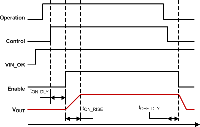
The start-up and shutdown function of the device is controlled by operation command, control pin or input voltage. Figure 19 shows the TPS40425 device is controlled by both operation command and control pin. A turn-on delay and turn-off delay can be added via PMBus commands.
NOTE
If the device turns off due to a turn-off delay time, any attempt to turn on the device before the turn-off delay time expires should be avoided. The device is available to be turned on only after the turn-off delay time expires and the device has been turned off.
For 3-phase and 4-phase configurations, the turn-on delay of both controllers must be programmed to the same value. The same requirement is for turn-off delay.
 Figure 19. Device Controlled by Both OPERATION and CONTROL