SLUS600E April 2004 – December 2014 TPS51100
PRODUCTION DATA.
- 1 Features
- 2 Applications
- 3 Description
- 4 Revision History
- 5 Pin Configuration and Functions
- 6 Specifications
- 7 Detailed Description
- 8 Application and Implementation
- 9 Power Supply Recommendations
- 10Layout
- 11Device and Documentation Support
- 12Mechanical, Packaging, and Orderable Information
Package Options
Refer to the PDF data sheet for device specific package drawings
Mechanical Data (Package|Pins)
- DGQ|10
Thermal pad, mechanical data (Package|Pins)
- DGQ|10
Orderable Information
8 Application and Implementation
NOTE
Information in the following applications sections is not part of the TI component specification, and TI does not warrant its accuracy or completeness. TI’s customers are responsible for determining suitability of components for their purposes. Customers should validate and test their design implementation to confirm system functionality.
8.1 Application Information
The TPS51100 is typically used as a sink / source tracking termination regulator, witch converter a voltage from VTT.
8.2 Typical Application
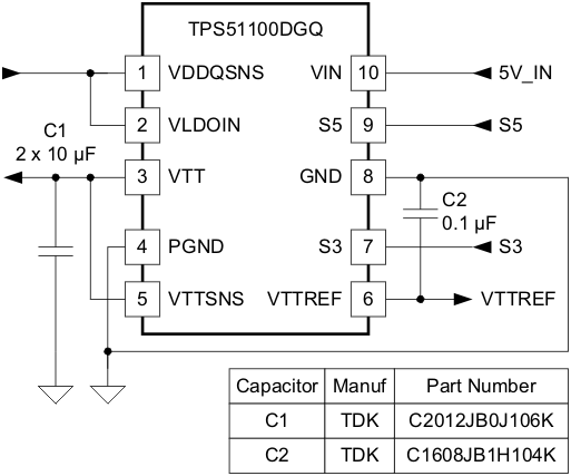 Figure 23. TPS51100 5-V Input / 1.8-V Output Reference Design
8.2.1 Design Requirements
Table 2. Design Parameters
| DESIGN PARAMETERS | EXAMPLE VALUE | |||
|---|---|---|---|---|
| VIN | 4.75 V to 5.25 V | |||
| VDDQSNS, VLDOIN | 1.8 V | |||
| Output Current | ±3 A | |||
8.2.2 Detailed Design Procedure
Table 3. Design Specifications
| REFERENCE DESIGNATOR | SPECIFICATION | MANUFACTURER | PART NUMBER | |
|---|---|---|---|---|
| C1 | 10-μf, 6.3-V, X5R, 2012 (0805) | TDK | C2012JB0J106K | |
| C2 | 0.1-μf, 50-V, X5R, 1608 (0603) | TDK | C1608JB1H104K | |
8.2.2.1 Output Capacitor
For stable operation, total capacitance of the VTT output terminal can be equal to or greater than 20 μF. Attach two 10-μF ceramic capacitors in parallel to minimize the effect of ESR and ESL. If the ESR is greater than 2 mΩ, insert an R-C filter between the output and the VTTSNS input to achieve loop stability. The R-C filter time constant should be almost the same or slightly lower than the time constant of the output capacitor and its ESR.
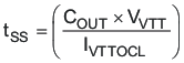
Soft-start duration, tSS, is also a function of this output capacitance. Where ITTOCL = 2.2 A (typ), tSS can be calculated as,
8.2.2.2 Input Capacitor
Depending on the trace impedance between the VLDOIN bulk power supply to the part, transient increase of source current is supplied mostly by the charge from the VLDOIN input capacitor. Use a 10-μF (or more) ceramic capacitor to supply this transient charge. Provide more input capacitance as more output capacitance is used at VTT. In general, use 1/2 COUT for the input.
8.2.2.3 VIN Capacitor
Add a ceramic capacitor with a value between 1 μF and 4.7 μF placed close to the VIN pin, to stabilize 5 V from any parasitic impedance from the supply.
8.2.3 Application Curves
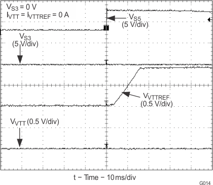 Figure 24. Start-Up Waveforms S5 Low-to-High
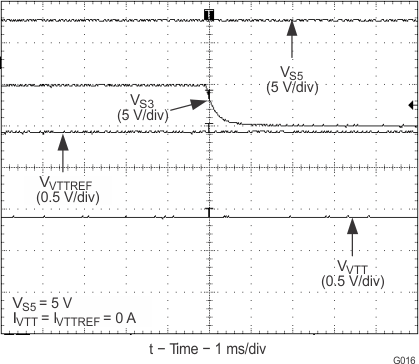 Figure 26. Shutdown Waveforms S3 High-to-Low
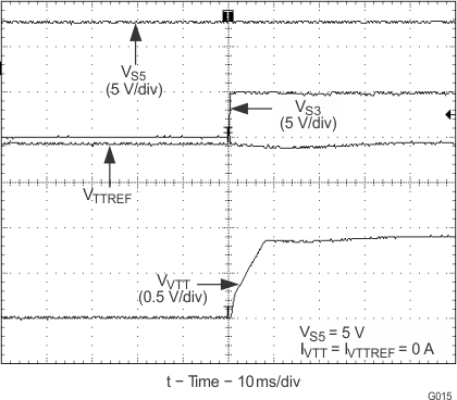 Figure 25. Start-Up Waveforms S3 Low-to-High