SLUS609J May   2004  – January 2018 TPS51116

PRODUCTION DATA.  

  1. Features
  2. Applications
  3. Description
    1.     Device Images
      1. 3.1 Typical Application
  4. Revision History
  5. Pin Configuration and Functions
    1.     Pin Functions
  6. Specifications
    1. 6.1 Absolute Maximum Ratings
    2. 6.2 ESD Ratings
    3. 6.3 Recommended Operating Conditions
    4. 6.4 Dissipation Ratings
    5. 6.5 Thermal Information
    6. 6.6 Electrical Characteristics
    7. 6.7 Typical Characteristics
  7. Detailed Description
    1. 7.1 Overview
    2. 7.2 Functional Block Diagram
    3. 7.3 Feature Description
      1. 7.3.1  VDDQ SMPS, Light Load Condition
      2. 7.3.2  Low-Side Driver
      3. 7.3.3  High-Side Driver
      4. 7.3.4  Current Sensing Scheme
      5. 7.3.5  PWM Frequency and Adaptive On-Time Control
      6. 7.3.6  VDDQ Output Voltage Selection
      7. 7.3.7  VTT Linear Regulator and VTTREF
      8. 7.3.8  Controling Outputs Using the S3 and S5 Pins
      9. 7.3.9  Soft-Start Function and Powergood Status
      10. 7.3.10 VDDQ and VTT Discharge Control
      11. 7.3.11 Current Protection for VDDQ
      12. 7.3.12 Current Protection for VTT
      13. 7.3.13 Overvoltage and Undervoltage Protection for VDDQ
      14. 7.3.14 Undervoltage Lockout (UVLO) Protection, V5IN (PWP), V5FILT (RGE)
      15. 7.3.15 Input Capacitor, V5IN (PWP), V5FILT (RGE)
      16. 7.3.16 Thermal Shutdown
    4. 7.4 Device Functional Modes
      1. 7.4.1 VDDQ SMPS, Dual PWM Operation Modes
      2. 7.4.2 Current Mode Operation
      3. 7.4.3 D-CAP™ Mode Operation
  8. Application and Implementation
    1. 8.1 Application Information
    2. 8.2 DDR3 Application With Current Mode
      1. 8.2.1 Design Requirements
      2. 8.2.2 Detailed Design Procedure
        1. 8.2.2.1 Pin Connections
        2. 8.2.2.2 Choose the inductor
        3. 8.2.2.3 Choose rectifying (low-side) MOSFET
        4. 8.2.2.4 Choose output capacitance
        5. 8.2.2.5 Determine f0 and calculate RC
        6. 8.2.2.6 Calculate CC2
        7. 8.2.2.7 Calculate CC.
        8. 8.2.2.8 Determine the value of R1 and R2.
      3. 8.2.3 Application Curves
    3. 8.3 DDR3 Application With D−CAP™ Mode
      1. 8.3.1 Design Requirements
      2. 8.3.2 Detailed Design Procedure
        1. 8.3.2.1 Pin Connections
        2. 8.3.2.2 Choose the Components
      3. 8.3.3 Application Curves
  9. Power Supply Recommendations
  10. 10Layout
    1. 10.1 Layout Guidelines
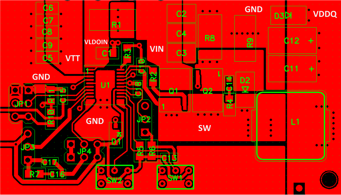
    2. 10.2 Layout Example
  11. 11Device and Documentation Support
    1. 11.1 Receiving Notification of Documentation Updates
    2. 11.2 Community Resources
    3. 11.3 Trademarks
    4. 11.4 Electrostatic Discharge Caution
    5. 11.5 Glossary
  12. 12Mechanical, Packaging, and Orderable Information

Package Options

Refer to the PDF data sheet for device specific package drawings

Mechanical Data (Package|Pins)
  • RGE|24
  • PWP|20
Thermal pad, mechanical data (Package|Pins)
Orderable Information

Layout Example

TPS51116 layout_slus609.pngFigure 47. Layout