SLVS616C November 2005 – December 2014 TPS51124
PRODUCTION DATA.
- 1 Features
- 2 Applications
- 3 Description
- 4 Revision History
- 5 Pin Configuration and Functions
- 6 Specifications
- 7 Detailed Description
- 8 Application and Implementation
- 9 Power Supply Recommendations
- 10Layout
- 11Device and Documentation Support
- 12Mechanical, Packaging, and Orderable Information
Package Options
Mechanical Data (Package|Pins)
- RGE|24
Thermal pad, mechanical data (Package|Pins)
- RGE|24
Orderable Information
1 Features
- High Efficiency, Low-Power Consumption, Shutdowns to <1 μA
- Fixed Frequency Emulated On-Time Control, Frequency Selectable From Three Options
- D-CAP™ Mode Enables Fast Transient Response
- Auto-Skip Mode
- Less Than 1% Initial Reference Accuracy
- Low Output Ripple
- Wide Input Voltage Range: 3 V to 28 V
- Output Voltage Range: 0.76 V to 5.5 V
- Low-Side RDS(ON) Loss-less Current Sensing
- Adaptive Gate Drivers With Integrated Boost Diode
- Internal 1.2-ms Voltage-Servo Soft-Start
- Powergood Signals for Each Channel With Delay Timer
- Output Discharge During Disable, Fault
2 Applications
Notebook I/O and Low-Voltage System Bus
3 Description
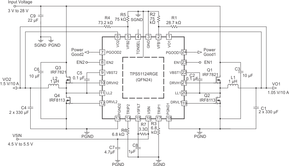
The TPS51124 is a dual, adaptive on-time D-CAP™ mode synchronous buck controller. The part enables system designers to cost effectively complete the suite of notebook power bus regulators with the absolute lowest external component count and lowest standby consumption. The fixed frequency emulated adaptive on-time control supports seamless operation between PWM mode at heavy load condition and reduced frequency operation at light load for high efficiency down to milliampere range. The main control loop for the TPS51124 uses the D-CAP mode that optimized for low ESR output capacitors such as POSCAP or SP-CAP promises fast transient response with no external compensation. Simple and separate power good signals for each channel allow flexibility of power sequencing. The part provides a convenient and efficient operation with supply input voltages (V5IN, V5FILT) ranging from 4.5 V to 5.5 V, conversion voltages (drain voltage for the synchronous high-side MOSFET) from 3 V to 28 V and output voltages from 0.76 V to 5.5 V.
The TPS51124 is available in 24-pin VQFN package specified from –40°C to 85°C ambient temperature range.
Device Information(1)
| PART NUMBER | PACKAGE | BODY SIZE (NOM) |
|---|---|---|
| TPS51124 | VQFN (24) | 4.00 mm × 4.00 mm |
- For all available packages, see the orderable addendum at the end of the datasheet.