SLUSAH1E MAY 2011 – July 2018 TPS51206
PRODUCTION DATA.
- 1 Features
- 2 Applications
- 3 Description
- 4 Revision History
- 5 Pin Configuration and Functions
- 6 Specifications
- 7 Detailed Description
- 8 Application and Implementation
- 9 Power Supply Recommendations
- 10Layout
- 11Device and Documentation Support
- 12Mechanical, Packaging, and Orderable Information
Package Options
Mechanical Data (Package|Pins)
- DSQ|10
Thermal pad, mechanical data (Package|Pins)
Orderable Information
6.6 Typical Characteristics
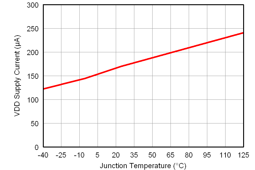 Figure 1. VDD Supply Current vs. Junction Temperature
 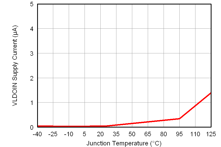 Figure 3. VLDOIN Supply Current vs. Junction Temperature
  Figure 5. VTTREF Load Regulation (0.9 V)
 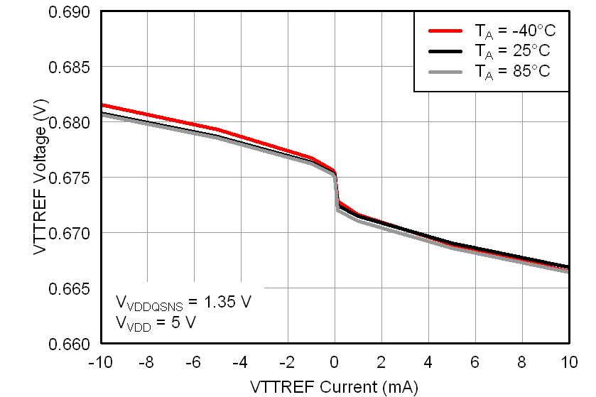 Figure 7. VTTREF Load Regulation (0.675 V)
 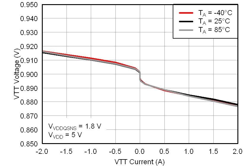 Figure 9. VTT Load Regulation (0.9 V)
 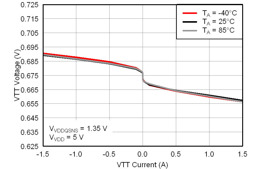 Figure 11. VTT Load Regulation (0.675 V)
 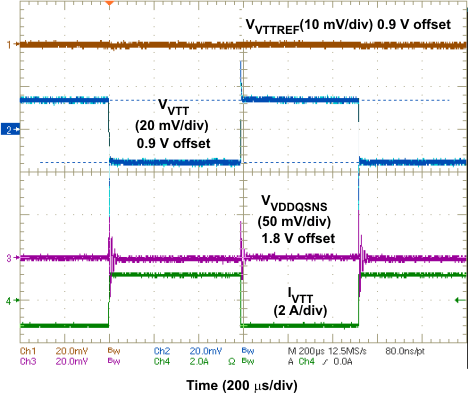 Figure 13. VTT Load Transient Response (0.9 V)
 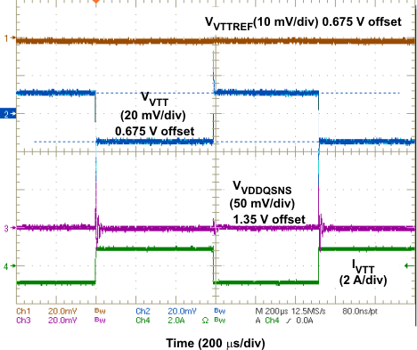 Figure 15. VTT Load Transient Response (0.675 V)
 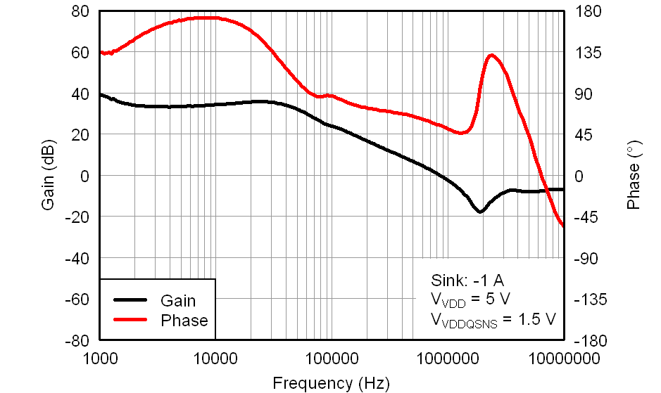 Figure 17. VTT (Sink: -1 A) Bode Plot (0.75 V)
 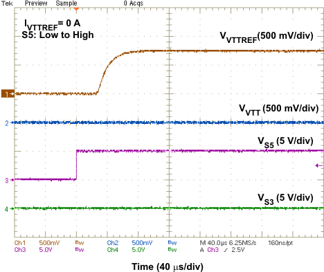 Figure 19. Start-Up Waveforms (S5: Low to High)
 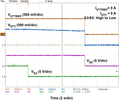 Figure 21. Shutdown Waveforms (S3/ S5: High to Low)
 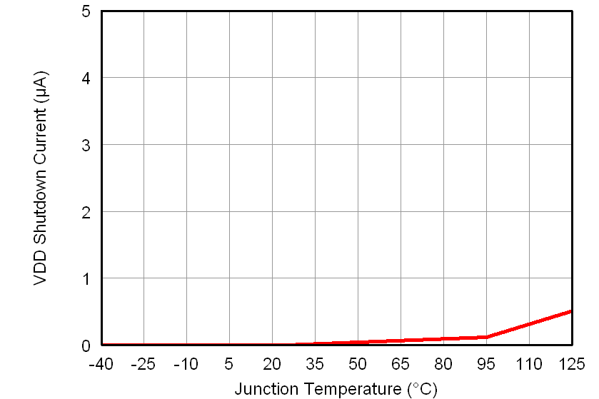 Figure 2. VDD Shutdown Current vs. Junction Temperature
 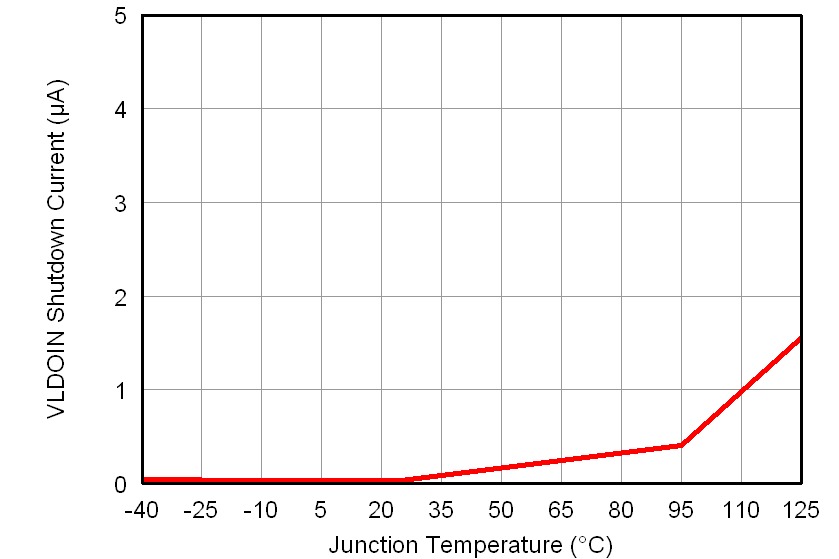 Figure 4. VLDOIN Shutdown Current vs. Junction Temperature
 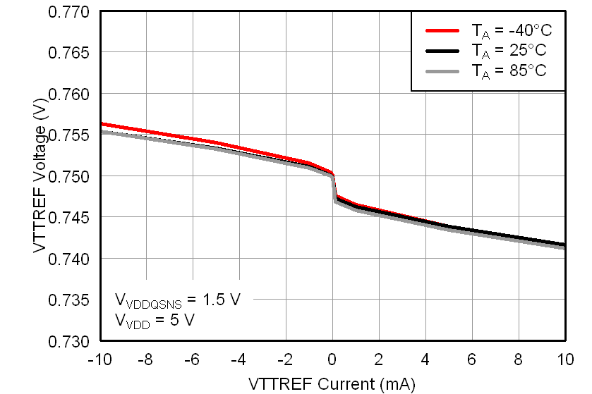 Figure 6. VTTREF Load Regulation (0.75 V)
 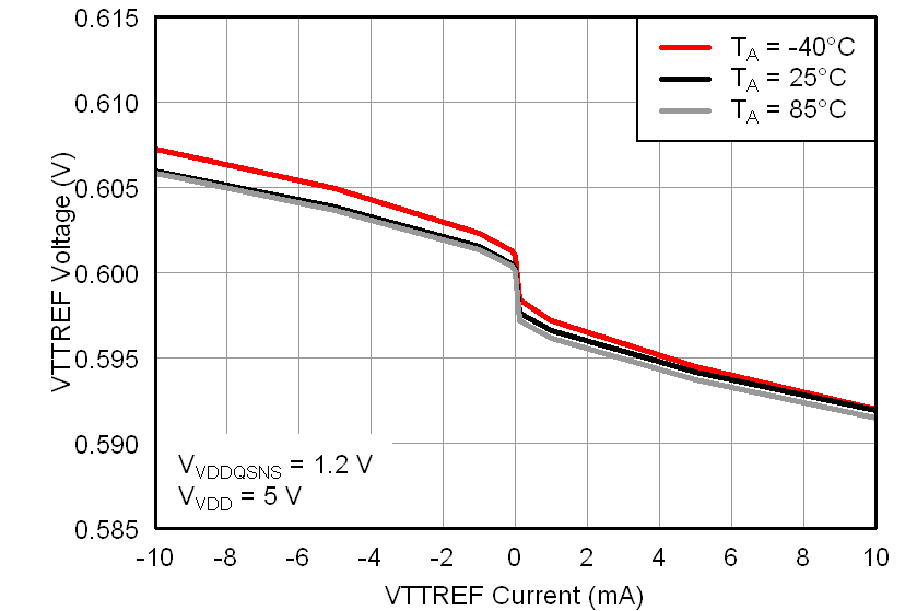 Figure 8. VTTREF Load Regulation (0.6 V)
  Figure 10. VTT Load Regulation (0.75 V)
 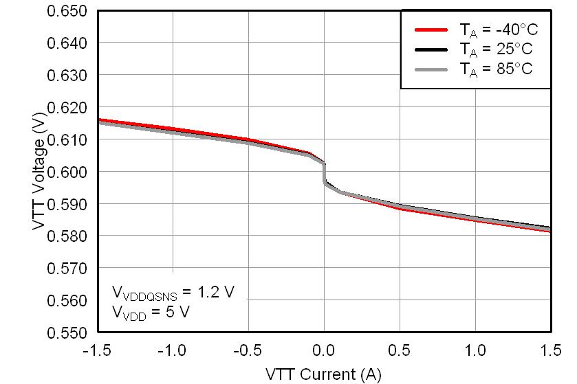 Figure 12. VTT Load Regulation (0.6 V)
 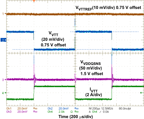 Figure 14. VTT Load Transient Response (0.75 V)
 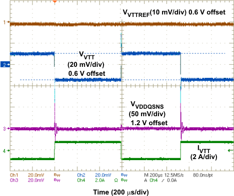 Figure 16. VTT Load Transient Response (0.6 V)
 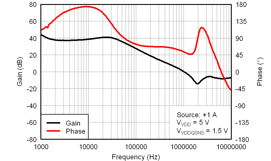 Figure 18. VTT (Source: +1 A) Bode Plot (0.75 V)
 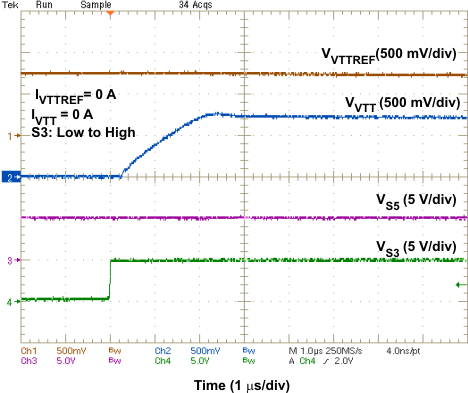 Figure 20. Start-Up Waveforms (S3: Low to High)
 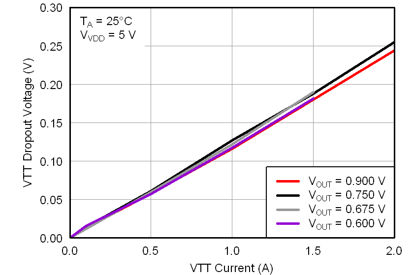 Figure 22. VTT Dropout Voltage