SLUSBA6B December 2012 – October 2015 TPS51604
PRODUCTION DATA.
- 1 Features
- 2 Applications
- 3 Description
- 4 Revision History
- 5 Pin Configuration and Functions
- 6 Specifications
- 7 Detailed Description
- 8 Application and Implementation
- 9 Power Supply Recommendations
- 10Layout
- 11Device and Documentation Support
- 12Mechanical, Packaging, and Orderable Information
Package Options
Mechanical Data (Package|Pins)
- DSG|8
Thermal pad, mechanical data (Package|Pins)
- DSG|8
Orderable Information
10 Layout
10.1 Layout Guidelines
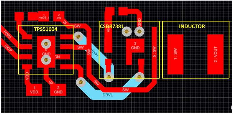
To improve the switching characteristics and design efficiency, these layout rules must be considered:
- Locate the driver as close as possible to the MOSFETs.
- Locate the VDD and bootstrap capacitors as close as possible to the driver.
- Pay special attention to the GND trace. Use the thermal pad of the package as the GND by connecting it to the GND pin. The GND trace or pad from the driver goes directly to the source of the MOSFET, but should not include the high current path of the main current flowing through the drain and source of the MOSFET.
- Use a similar rule for the switch-node as for the GND.
- Use wide traces for DRVH and DRVL closely following the related SW and GND traces. A width of between 80 and 100 mils is preferable where possible.
- Place the bypass capacitors as close as possible to the driver.
- Avoid PWM and enable traces going close to the SW and pad where high dV/dT voltage can induce significant noise into the relatively high-impedance leads.
A poor layout can decrease the reliability of the entire system.
10.2 Layout Example
 Figure 24. Layout Recommendation