SLUS851D October 2008 – October 2014 TPS54231
PRODUCTION DATA.
- 1 Features
- 2 Applications
- 3 Description
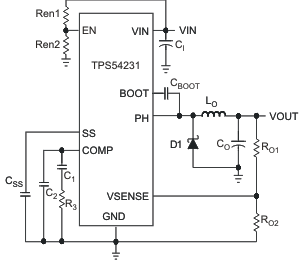
- 4 Simplified Schematic
- 5 Revision History
- 6 Pin Configuration and Functions
- 7 Specifications
-
8 Detailed Description
- 8.1 Overview
- 8.2 Functional Block Diagram
- 8.3
Feature Description
- 8.3.1 Fixed-Frequency PWM Control
- 8.3.2 Voltage Reference (Vref)
- 8.3.3 Bootstrap Voltage (BOOT)
- 8.3.4 Enable and Adjustable Input Undervoltage Lockout (VIN UVLO)
- 8.3.5 Programmable Slow Start Using SS Pin
- 8.3.6 Error Amplifier
- 8.3.7 Slope Compensation
- 8.3.8 Current-Mode Compensation Design
- 8.3.9 Overcurrent Protection and Frequency Shift
- 8.3.10 Overvoltage Transient Protection
- 8.3.11 Thermal Shutdown
- 8.4 Device Functional Modes
-
9 Application and Implementation
- 9.1 Application Information
- 9.2
Typical Application
- 9.2.1 Design Requirements
- 9.2.2 Detailed Design Procedure
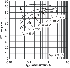
- 9.2.3 Application Curves
- 10Power Supply Recommendations
- 11Layout
- 12Device and Documentation Support
- 13Mechanical, Packaging, and Orderable Information
Package Options
Mechanical Data (Package|Pins)
- D|8
Thermal pad, mechanical data (Package|Pins)
Orderable Information
1 Features
- 3.5- to 28-V Input Voltage Range
- Adjustable Output Voltage Down to 0.8 V
- Integrated 80-mΩ High-Side MOSFET Supports up to 2 A Continuous Output Current
- High Efficiency at Light Loads with a Pulse Skipping Eco-mode™
- Fixed 570-kHz Switching Frequency
- Typical 1-μA Shutdown Quiescent Current
- Adjustable Slow-Start Limits Inrush Currents
- Programmable UVLO Threshold
- Overvoltage Transient Protection
- Cycle-by-Cycle Current Limit, Frequency Fold Back and Thermal Shutdown Protection
- Available in Easy-to-Use SOIC8 Package
- Supported by WEBENCH® Software Tool (www.TI.com/WEBENCH)
2 Applications
- Consumer Applications such as Set-Top Boxes, CPE Equipment, LCD Displays, Peripherals, and Battery Chargers
- Industrial and Car Audio Power Supplies
- 5-V, 12-V and 24-V Distributed Power Systems
3 Description
The TPS54231 device is a 2-V, 2-A non-synchronous buck converter that integrates a low RDS(on) high-side MOSFET. To increase efficiency at light loads, a pulse skipping Eco-mode™ feature is automatically activated. Furthermore, the 1-μA shutdown supply current allows the device to be used in battery powered applications. Current mode control with internal slope compensation simplifies the external compensation calculations and reduces component count while allowing the use of ceramic output capacitors. A resistor divider programs the hysteresis of the input undervoltage lockout. An overvoltage transient protection circuit limits voltage overshoots during startup and transient conditions. A cycle-by-cycle current limit scheme, frequency fold back and thermal shutdown protect the device and the load in the event of an overload condition. The TPS54231 device is available in an 8-pin SOIC package that has been internally optimized to improve thermal performance.
Device Information(1)
| PART NUMBER | PACKAGE | BODY SIZE (NOM) |
|---|---|---|
| TPS54231 | SOIC (8) | 4.90 mm × 3.90 mm |
- For all available packages, see the orderable addendum at the end of the datasheet.
4 Simplified Schematic
Efficiency