SLVSCD5D November 2014 – February 2016 TPS54335-1A , TPS54335A , TPS54336A
PRODUCTION DATA.
- 1 Features
- 2 Applications
- 3 Description
- 4 Revision History
- 5 Pin Configuration and Functions
- 6 Specifications
-
7 Detailed Description
- 7.1 Overview
- 7.2 Functional Block Diagram
- 7.3
Feature Description
- 7.3.1 Fixed-Frequency PWM Control
- 7.3.2 Light-Load Operation
- 7.3.3 Voltage Reference
- 7.3.4 Adjusting the Output Voltage
- 7.3.5 Enabling and Adjusting Undervoltage Lockout
- 7.3.6 Error Amplifier
- 7.3.7 Slope Compensation and Output Current
- 7.3.8 Safe Startup into Pre-Biased Outputs
- 7.3.9 Bootstrap Voltage (BOOT)
- 7.3.10 Adjustable Switching Frequency (TPS54335A Only)
- 7.3.11 Soft-Start (TPS54336A Only)
- 7.3.12 Output Overvoltage Protection (OVP)
- 7.3.13 Overcurrent Protection
- 7.3.14 Thermal Shutdown
- 7.3.15 Small-Signal Model for Loop Response
- 7.3.16 Simple Small-Signal Model for Peak Current-Mode Control
- 7.3.17 Small-Signal Model for Frequency Compensation
- 7.4 Device Functional Modes
-
8 Application and Implementation
- 8.1 Application Information
- 8.2
Typical Applications
- 8.2.1 Design Requirements
- 8.2.2 Detailed Design Procedure
- 8.2.3 Application Curves
- 8.2.4 TPS54336A Typical Application
- 9 Power Supply Recommendations
- 10Layout
- 11Device and Documentation Support
- 12Mechanical, Packaging, and Orderable Information
Package Options
Refer to the PDF data sheet for device specific package drawings
Mechanical Data (Package|Pins)
- DRC|10
- DDA|8
Thermal pad, mechanical data (Package|Pins)
Orderable Information
10 Layout
10.1 Layout Guidelines
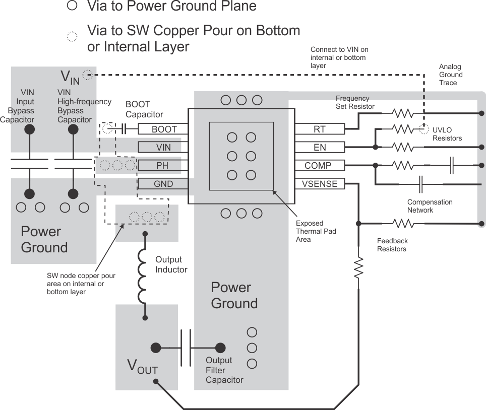
The VIN pin should be bypassed to ground with a low-ESR ceramic bypass capacitor. Care should be taken to minimize the loop area formed by the bypass capacitor connection, the VIN pin, and the GND pin of the IC. The typical recommended bypass capacitance is 10-μF ceramic with a X5R or X7R dielectric and the optimum placement is closest to the VIN and GND pins of the device. See Figure 55 for a PCB layout example. The GND pin should be tied to the PCB ground plane at the pin of the IC. To facilitate close placement of the input bypass capacitors, the PH pin should be routed to a small copper area directly adjacent to the pin. Use vias to route the PH signal to the bottom side or an inner layer. If necessary, allow the top-side copper area to extend slightly under the body of the closest input bypass capacitor. Make the copper trace on the bottom or internal layer short and wide as practical to reduce EMI issues. Connect the trace with vias back to the top side to connect with the output inductor as shown after the GND pin. In the same way use a bottom or internal layer trace to route the PH signal across the VIN pin to connect to the boot capacitor as shown. Make the circulating loop from the PH pin to the output inductor and output capacitors and then back to GND as tight as possible while preserving adequate etch width to reduce conduction losses in the copper . For operation at a full rated load, the ground area near the IC must provide adequate heat dissipating area. Connect the exposed thermal pad to the bottom or internal layer ground plane using vias as shown. Additional vias may be used adjacent to the IC to tie top-side copper to the internal or bottom layer copper. The additional external components can be placed approximately as shown. Use a separate ground trace to connect the feedback, compensation, UVLO, and RT (SS for TPS54336A) returns. Connect this ground trace to the main power ground at a single point to minimize circulating currents. Obtaining acceptable performance with alternate layout schemes is possible; however this layout has been shown to produce good results and is intended as a guideline.
10.2 Layout Example

NOTE:
Pin 8 for the TPS54336A device is SS. Connect an SS capacitor instead of an RT resistor from pin 8 to GND.