SLVSDV8 July 2017 TPS54424
PRODUCTION DATA.
- 1 Features
- 2 Applications
- 3 Description
- 4 Revision History
- 5 Pin Configuration and Functions
- 6 Specifications
-
7 Detailed Description
- 7.1 Overview
- 7.2 Functional Block Diagram
- 7.3
Feature Description
- 7.3.1 Fixed Frequency PWM Control
- 7.3.2 Continuous Conduction Mode Operation (CCM)
- 7.3.3 VIN Pins and VIN UVLO
- 7.3.4 Voltage Reference and Adjusting the Output Voltage
- 7.3.5 Error Amplifier
- 7.3.6 Enable and Adjustable UVLO
- 7.3.7 Soft Start and Tracking
- 7.3.8 Safe Start-up into Pre-Biased Outputs
- 7.3.9 Power Good
- 7.3.10 Sequencing (SS/TRK)
- 7.3.11 Adjustable Switching Frequency (RT Mode)
- 7.3.12 Synchronization (CLK Mode)
- 7.3.13 Bootstrap Voltage and 100% Duty Cycle Operation (BOOT)
- 7.3.14 Output Overvoltage Protection (OVP)
- 7.3.15 Overcurrent Protection
- 7.4 Device Functional Modes
-
8 Application and Implementation
- 8.1 Application Information
- 8.2
Typical Application
- 8.2.1 Design Requirements
- 8.2.2
Detailed Design Procedure
- 8.2.2.1 Custom Design With WEBENCH® Tools
- 8.2.2.2 Switching Frequency
- 8.2.2.3 Output Inductor Selection
- 8.2.2.4 Output Capacitor
- 8.2.2.5 Input Capacitor
- 8.2.2.6 Output Voltage Resistors Selection
- 8.2.2.7 Soft-start Capacitor Selection
- 8.2.2.8 Undervoltage Lockout Set Point
- 8.2.2.9 Bootstrap Capacitor Selection
- 8.2.2.10 PGOOD Pull-up Resistor
- 8.2.2.11 Compensation
- 8.2.3 Application Curves
- 9 Power Supply Recommendations
- 10Layout
- 11Device and Documentation Support
- 12Mechanical, Packaging, and Orderable Information
Package Options
Refer to the PDF data sheet for device specific package drawings
Mechanical Data (Package|Pins)
- RNV|18
Thermal pad, mechanical data (Package|Pins)
Orderable Information
3 Description
The TPS54424 is a full-featured 17-V (19-V maximum), 4-A synchronous step-down DC/DC converter in a 3.5 mm × 3.5 mm HotRod™ QFN package.
The device is optimized for small solution size through high efficiency and integrating the high-side and low-side MOSFETs. Further space savings are achieved through peak current mode control, which reduces component count, and by selecting a high switching frequency, reducing the inductor footprint.
The peak current mode control simplifies the loop compensation and provides fast transient response. Cycle-by-cycle peak current limiting on the high-side and low-side sourcing current limit protects the device in overload situations. Hiccup limits MOSFET power dissipation if a short circuit or over loading fault persists.
A power good supervisor circuit monitors the regulator output. The PGOOD pin is an open-drain output and goes high impedance when the output voltage is in regulation. An internal deglitch time prevents the PGOOD pin from pulling low unless a fault has occurred.
A dedicated EN pin can be used to control the regulator on/off and adjust the input undervoltage lockout. The output voltage start-up ramp is controlled by the SS/TRK pin, which allows operation as either a standalone power supply or in tracking situations.
Device Information(1)
| PART NUMBER | PACKAGE | BODY SIZE (NOM) |
|---|---|---|
| TPS54424 | RNV (18) | 3.50 mm × 3.50 mm |
- For all available packages, see the orderable addendum at the end of the data sheet.
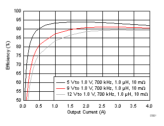
Efficiency
