SLVS949F May 2009 – May 2017 TPS54620
PRODUCTION DATA.
- 1 Features
- 2 Applications
- 3 Description
- 4 Revision History
- 5 Pin Configurations and Functions
- 6 Specifications
-
7 Detailed Description
- 7.1 Overview
- 7.2 Functional Block Diagram
- 7.3
Feature Description
- 7.3.1 Fixed Frequency PWM Control
- 7.3.2 Continuous Current Mode Operation (CCM)
- 7.3.3 VIN and Power VIN Pins (VIN and PVIN)
- 7.3.4 Voltage Reference
- 7.3.5 Adjusting the Output Voltage
- 7.3.6 Safe Start-Up into Prebiased Outputs
- 7.3.7 Error Amplifier
- 7.3.8 Slope Compensation
- 7.3.9 Enable and Adjusting Undervoltage Lockout
- 7.3.10 Adjustable Switching Frequency and Synchronization (RT/CLK)
- 7.3.11 Slow Start (SS/TR)
- 7.3.12 Power Good (PWRGD)
- 7.3.13 Output Overvoltage Protection (OVP)
- 7.3.14 Overcurrent Protection
- 7.3.15 Thermal Shutdown
- 7.3.16 Small Signal Model for Loop Response
- 7.3.17 Simple Small Signal Model for Peak Current Mode Control
- 7.3.18 Small Signal Model for Frequency Compensation
- 7.4 Device Functional Modes
-
8 Application and Implementation
- 8.1 Application Information
- 8.2
Typical Application
- 8.2.1 Design Requirements
- 8.2.2
Detailed Design Procedures
- 8.2.2.1 Custom Design With WEBENCH Tools
- 8.2.2.2 Operating Frequency
- 8.2.2.3 Output Inductor Selection
- 8.2.2.4 Output Capacitor Selection
- 8.2.2.5 Input Capacitor Selection
- 8.2.2.6 Slow-Start Capacitor Selection
- 8.2.2.7 Bootstrap Capacitor Selection
- 8.2.2.8 Undervoltage Lockout Set Point
- 8.2.2.9 Output Voltage Feedback Resistor Selection
- 8.2.2.10 Compensation Component Selection
- 8.2.2.11 Fast Transient Considerations
- 8.2.3 Application Curves
- 9 Power Supply Recommendations
- 10Layout
- 11Device and Documentation Support
- 12Mechanical, Packaging, and Orderable Information
Package Options
Refer to the PDF data sheet for device specific package drawings
Mechanical Data (Package|Pins)
- RHL|14
- RGY|14
Thermal pad, mechanical data (Package|Pins)
Orderable Information
7 Detailed Description
7.1 Overview
The device is a 17-V, 6-A, synchronous step-down (buck) converter with two integrated n-channel MOSFETs. To improve performance during line and load transients, the device implements a constant frequency peak current mode control that also simplifies external frequency compensation. The wide switching frequency of 200 kHz to 1600 kHz allows for efficiency and size optimization when selecting the output filter components. The switching frequency is adjusted using a resistor-to-ground on the RT/CLK pin. The device also has an internal phase lock loop (PLL) controlled by the RT/CLK pin that can be used to synchronize the switching cycle to the falling edge of an external system clock.
The device has been designed for safe monotonic start-up into prebiased loads. The default start-up is when VIN is typically 4.0 V. The EN pin has an internal pullup current source that can be used to adjust the input voltage undervoltage lockout (UVLO) with two external resistors. In addition, the EN pin can be floating for the device to operate with the internal pullup current. The total operating current for the device is approximately 600 μA when not switching and under no load. When the device is disabled, the supply current is typically less than 2 μA.
The integrated MOSFETs allow for high efficiency power supply designs with continuous output currents up to 6 amperes. The MOSFETs have been sized to optimize efficiency for lower duty cycle applications.
The device reduces the external component count by integrating the boot recharge circuit. The bias voltage for the integrated high-side MOSFET is supplied by a capacitor between the BOOT and PH pins. The boot capacitor voltage is monitored by a BOOT to PH UVLO (BOOT-PH UVLO) circuit allowing PH pin to be pulled low to recharge the boot capacitor. The device can operate at 100% duty cycle as long as the boot capacitor voltage is higher than the preset BOOT-PH UVLO threshold which is typically 2.1 V. The output voltage can be stepped down to as low as the 0.8-V voltage reference (Vref).
The device has a power good comparator (PWRGD) with hysteresis which monitors the output voltage through the VSENSE pin. The PWRGD pin is an open-drain MOSFET which is pulled low when the VSENSE pin voltage is less than 91% or greater than 109% of the reference voltage Vref and asserts high when the VSENSE pin voltage is 94% to 106% of the Vref.
The SS/TR (slow start/tracking) pin is used to minimize inrush currents or provide power supply sequencing during power up. A small value capacitor or resistor divider should be coupled to the pin for slow start or critical power supply sequencing requirements.
The device is protected from output overvoltage, overload, and thermal fault conditions. The device minimizes excessive output overvoltage transients by taking advantage of the overvoltage circuit power good comparator. When the overvoltage comparator is activated, the high-side MOSFET is turned off and prevented from turning on until the VSENSE pin voltage is lower than 106% of the Vref. The device implements both high-side MOSFET overload protection and bidirectional low-side MOSFET overload protections which help control the inductor current and avoid current runaway. The device also shuts down if the junction temperature is higher than thermal shutdown trip point. The device is restarted under control of the slow-start circuit automatically when the junction temperature drops 10°C typically below the thermal shutdown trip point.
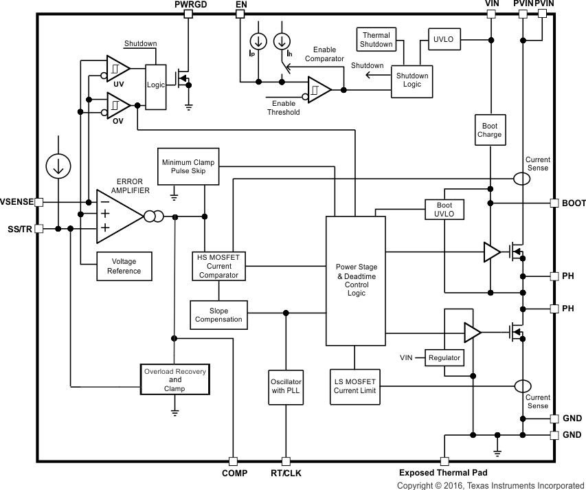
7.2 Functional Block Diagram
7.3 Feature Description
7.3.1 Fixed Frequency PWM Control
The device uses a adjustable fixed frequency, peak current mode control. The output voltage is compared through external resistors on the VSENSE pin to an internal voltage reference by an error amplifier which drives the COMP pin. An internal oscillator initiates the turnon of the high-side power switch. The error amplifier output is converted into a current reference which compares to the high-side power switch current. When the power switch current reaches current reference generated by the COMP voltage level the high-side power switch is turned off and the low-side power switch is turned on.
7.3.2 Continuous Current Mode Operation (CCM)
As a synchronous buck converter, the device normally works in CCM (Continuous Conduction Mode) under all load conditions.
7.3.3 VIN and Power VIN Pins (VIN and PVIN)
The device allows for a variety of applications by using the VIN and PVIN pins together or separately. The VIN pin voltage supplies the internal control circuits of the device. The PVIN pin voltage provides the input voltage to the power converter system.
If tied together, the input voltage for VIN and PVIN can range from 4.5 V to 17 V. If using the VIN separately from PVIN, the VIN pin must be between 4.5 V and 17 V, and the PVIN pin can range from as low as 1.6 V to 17 V. A voltage divider connected to the EN pin can adjust the either input voltage UVLO appropriately. Adjusting the input voltage UVLO on the PVIN pin helps to provide consistent power up behavior.
7.3.4 Voltage Reference
The voltage reference system produces a precise ±1% voltage reference over temperature by scaling the output of a temperature stable bandgap circuit.
7.3.5 Adjusting the Output Voltage
The output voltage is set with a resistor divider from the output (VOUT) to the VSENSE pin. TI recommends using 1% tolerance or better divider resistors. Referring to the application schematic of Figure 34, start with a 10 kΩ for R6 and use Equation 1 to calculate R5. To improve efficiency at light loads consider using larger value resistors. If the values are too high the regulator is more susceptible to noise and voltage errors from the VSENSE input current are noticeable.

where
- Vref = 0.8V
The minimum output voltage and maximum output voltage can be limited by the minimum on time of the high-side MOSFET and bootstrap voltage (BOOT-PH voltage) respectively. More discussions are located in Minimum Output Voltage and Bootstrap Voltage (BOOT) and Low Dropout Operation.
7.3.6 Safe Start-Up into Prebiased Outputs
The device has been designed to prevent the low-side MOSFET from discharging a prebiased output. During monotonic prebiased start-up, the low-side MOSFET is not allowed to sink current until the SS/TR pin voltage is higher than 1.4 V.
7.3.7 Error Amplifier
The device uses a transconductance error amplifier. The error amplifier compares the VSENSE pin voltage to the lower of the SS/TR pin voltage or the internal 0.8-V voltage reference. The transconductance of the error amplifier is 1300 μA/V during normal operation. The frequency compensation network is connected between the COMP pin and ground.
7.3.8 Slope Compensation
The device adds a compensating ramp to the switch current signal. This slope compensation prevents sub-harmonic oscillations. The available peak inductor current remains constant over the full duty cycle range.
7.3.9 Enable and Adjusting Undervoltage Lockout
The EN pin provides electrical on/off control of the device. When the EN pin voltage exceeds the threshold voltage, the device starts operation. If the EN pin voltage is pulled below the threshold voltage, the regulator stops switching and enters low Iq state.
The EN pin has an internal pullup current source, allowing the user to float the EN pin for enabling the device. If an application requires controlling the EN pin, use either open-drain or open-collector output logic to interface with the pin.
The device implements internal UVLO circuitry on the VIN pin. The device is disabled when the VIN pin voltage falls below the internal VIN UVLO threshold. The internal VIN UVLO threshold has a hysteresis of 150 mV.
If an application requires either a higher UVLO threshold on the VIN pin or a secondary UVLO on the PVIN in split-rail applications, then the EN pin can be configured as shown in Figure 17, Figure 18, and Figure 19. When using the external UVLO function, TI recommends setting the hysteresis to be greater than 500 mV.
The EN pin has a small pullup current Ip which sets the default state of the pin to enable when no external components are connected. The pullup current is also used to control the voltage hysteresis for the UVLO function because it increases by Ih when the EN pin crosses the enable threshold. The UVLO thresholds can be calculated using Equation 2 and Equation 3.
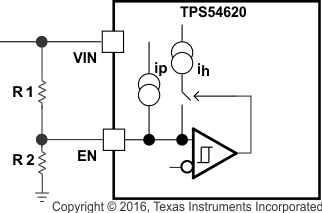 Figure 17. Adjustable VIN Undervoltage Lockout
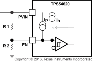 Figure 18. Adjustable PVIN Undervoltage Lockout, VIN ≥ 4.5 V
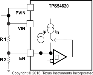 Figure 19. Adjustable VIN and PVIN Undervoltage Lockout
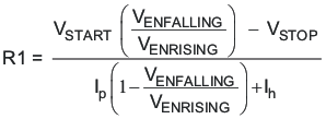

where
- Ih = 3.4 μA
- Ip = 1.15 μA
- VENRISING = 1.21 V
- VENFALLING = 1.17 V
7.3.10 Adjustable Switching Frequency and Synchronization (RT/CLK)
The RT/CLK pin can be used to set the switching frequency of the device in two modes.
In RT mode, a resistor (RT resistor) is connected between the RT/CLK pin and GND. The switching frequency of the device is adjustable from 200 kHz to 1600 kHz by placing a maximum of 240 kΩ and minimum of 29 kΩ, respectively. In CLK mode, an external clock is connected directly to the RT/CLK pin. The device is synchronized to the external clock frequency with PLL.
The CLK mode overrides the RT mode. The device is able to detect the proper mode automatically and switch from the RT mode to CLK mode.
7.3.11 Slow Start (SS/TR)
The device uses the lower voltage of the internal voltage reference or the SS/TR pin voltage as the reference voltage and regulates the output accordingly. A capacitor on the SS/TR pin to ground implements a slow-start time. The device has an internal pullup current source of 2.3 μA that charges the external slow-start capacitor. The calculations for the slow-start time (Tss, 10% to 90%) and slow-start capacitor (Css) are shown in Equation 4. The voltage reference (Vref) is 0.8 V and the slow-start charge current (Iss) is 2.3 μA.

When the input UVLO is triggered, the EN pin is pulled below 1.21 V, or a thermal shutdown event occurs, the device stops switching and enters low current operation. At the subsequent power up when the shutdown condition is removed, the device does not start switching until it has discharged its SS/TR pin to ground ensuring proper soft-start behavior.
7.3.12 Power Good (PWRGD)
The PWRGD pin is an open-drain output. When the VSENSE pin is between 94% and 106% of the internal voltage reference the PWRGD pin pulldown is deasserted and the pin floats. TI recommends using a pullup resistor between the values of 10 kΩ and 100 kΩ to a voltage source that is 5.5 V or less. The PWRGD is in a defined state when the VIN input voltage is greater than 1 V but with reduced current sinking capability. The PWRGD achieves full current sinking capability when the VIN input voltage is above 4.5 V.
The PWRGD pin is pulled low when VSENSE is lower than 91% or greater than 109% of the nominal internal reference voltage. Also, if the PWRGD is pulled low and the input UVLO or thermal shutdown are asserted, the EN pin is pulled low or the SS/TR pin is set below 1.4 V.
7.3.13 Output Overvoltage Protection (OVP)
The device incorporates an output overvoltage protection (OVP) circuit to minimize output voltage overshoot. For example, when the power supply output is overloaded the error amplifier compares the actual output voltage to the internal reference voltage. If the VSENSE pin voltage is lower than the internal reference voltage for a considerable time, the output of the error amplifier demands maximum output current. When the condition is removed, the regulator output rises and the error amplifier output transitions to the steady-state voltage. In some applications with small output capacitance, the power supply output voltage can respond faster than the error amplifier. This leads to the possibility of an output overshoot. The OVP feature minimizes the overshoot by comparing the VSENSE pin voltage to the OVP threshold. If the VSENSE pin voltage is greater than the OVP threshold the high-side MOSFET is turned off preventing current from flowing to the output and minimizing output overshoot. When the VSENSE voltage drops lower than the OVP threshold, the high-side MOSFET is allowed to turn on at the next clock cycle.
7.3.14 Overcurrent Protection
The device is protected from overcurrent conditions by cycle-by-cycle current limiting on both the high-side MOSFET and the low-side MOSFET.
7.3.14.1 High-Side MOSFET Overcurrent Protection
The device implements current mode control which uses the COMP pin voltage to control the turn off of the high-side MOSFET and the turn on of the low-side MOSFET on a cycle-by-cycle basis. Each cycle the switch current and the current reference generated by the COMP pin voltage are compared, when the peak switch current intersects the current reference the high-side switch is turned off.
7.3.14.2 Low-Side MOSFET Overcurrent Protection
While the low-side MOSFET is turned on its conduction current is monitored by the internal circuitry. During normal operation the low-side MOSFET sources current to the load. At the end of every clock cycle, the low-side MOSFET sourcing current is compared to the internally set low-side sourcing current limit. If the low-side sourcing current is exceeded the high-side MOSFET is not turned on and the low-side MOSFET stays on for the next cycle. The high-side MOSFET is turned on again when the low-side current is below the low-side sourcing current limit at the start of a cycle.
The low-side MOSFET may also sink current from the load. If the low-side sinking current limit is exceeded the low-side MOSFET is turned off immediately for the rest of that clock cycle. In this scenario both MOSFETs are off until the start of the next cycle.
7.3.15 Thermal Shutdown
The internal thermal shutdown circuitry forces the device to stop switching if the junction temperature exceeds 175°C typically. The device reinitiates the power-up sequence when the junction temperature drops below 165°C typically.
7.3.16 Small Signal Model for Loop Response
Figure 20 shows an equivalent model for the device control loop which can be modeled in a circuit simulation program to check frequency response and transient responses. The error amplifier is a transconductance amplifier with a gm of 1300 μA/V. The error amplifier can be modeled using an ideal voltage controlled current source. The resistor Roea (2.38 MΩ) and capacitor Coea (20.7 pF) model the open-loop gain and frequency response of the error amplifier. The 1-mV AC voltage source between the nodes a and b effectively breaks the control loop for the frequency response measurements. Plotting a/c and c/b show the small signal responses of the power stage and frequency compensation respectively. Plotting a/b shows the small signal response of the overall loop. The dynamic loop response can be checked by replacing the RL with a current source with the appropriate load step amplitude and step rate in a time domain analysis.
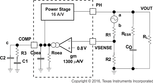 Figure 20. Small Signal Model for Loop Response
7.3.17 Simple Small Signal Model for Peak Current Mode Control
Figure 21 is a simple small signal model that can be used to understand how to design the frequency compensation. The device power stage can be approximated to a voltage-controlled current source (duty cycle modulator) supplying current to the output capacitor and load resistor. The control-to-output transfer function is shown in Equation 5 and consists of a DC gain, one dominant pole, and one ESR zero. The quotient of the change in switch current and the change in COMP pin voltage (node c in Figure 20) is the power stage transconductance (gmps), which is 16 A/V for the device. The DC gain of the power stage is the product of gmps, and the load resistance (RL) as shown in Equation 6 with resistive loads. As the load current increases, the DC gain decreases. This variation with load may seem problematic at first glance, but fortunately the dominant pole moves with load current (see Equation 7). The combined effect is highlighted by the dashed line in Figure 22. As the load current decreases, the gain increases and the pole frequency lowers, keeping the 0-dB crossover frequency the same for the varying load conditions, making it easier to design the frequency compensation.
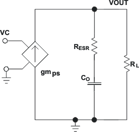 Figure 21. Simplified Small Signal Model for Peak Current Mode Control
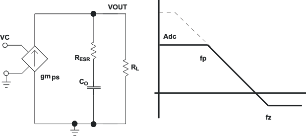 Figure 22. Simplified Frequency Response for Peak Current Mode Control
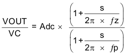

where
- gmps is the power stage gain (16 A/V).
- RL is the load resistance

where
- CO is the output capacitance.
- RL is the load resistance

where
- CO is the output capacitance.
- RESR is the equivalent series resistance of the output capacitor.
7.3.18 Small Signal Model for Frequency Compensation
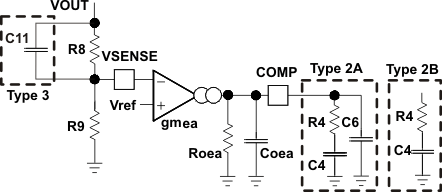
The device uses a transconductance amplifier for the error amplifier and readily supports two of the commonly used Type II compensation circuits and a Type III frequency compensation circuit, as shown in Figure 23. In Type 2A, one additional high frequency pole, C6, is added to attenuate high-frequency noise. In Type III, one additional capacitor, C11, is added to provide a phase boost at the crossover frequency. See Designing Type III Compensation for Current Mode Step-Down Converters (SLVA352) for a complete explanation of Type III compensation.
The design guidelines below are provided for advanced users who prefer to compensate using the general method. The below equations only apply to designs whose ESR zero is above the bandwidth of the control loop. This is usually true with ceramic output capacitors. See the Application Information section for a step-by-step design procedure using higher ESR output capacitors with lower ESR zero frequencies.
The general design guidelines for device loop compensation are as follows:
- Determine the crossover frequency, fc. A good starting point is 1/10th of the switching frequency, fsw.
- R4 can be determined by:
- gmea is the GM amplifier gain (1300 μA/V)
- gmps is the power stage gain (12 A/V)
- Vref is the reference voltage (0.8 V)
- Place a compensation zero at the dominant pole:

C4 can be determined by: - C6 is optional. It can be used to cancel the zero from the ESR (Equivalent Series Resistance) of the output capacitor Co.
- Type III compensation can be implemented with the addition of one capacitor, C11. This allows for slightly higher loop bandwidths and higher phase margins. If used, C11 is calculated from Equation 12.

where


7.4 Device Functional Modes
7.4.1 Adjustable Switching Frequency (RT Mode)
To determine the RT resistance for a given switching frequency, use Equation 13 or the curve in Figure 24. To reduce the solution size, one would set the switching frequency as high as possible, but tradeoffs of the supply efficiency and minimum controllable on-time must be considered.

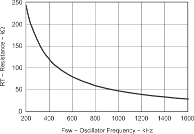 Figure 24. RT Set Resistor vs Switching Frequency
7.4.2 Synchronization (CLK Mode)
An internal Phase Locked Loop (PLL) has been implemented to allow synchronization between 200 kHz and 1600 kHz, and to easily switch from RT mode to CLK mode.
To implement the synchronization feature, connect a square wave clock signal to the RT/CLK pin with a duty cycle between 20% to 80%. The clock signal amplitude must transition lower than 0.8 V and higher than 2.0 V. The start of the switching cycle is synchronized to the falling edge of RT/CLK pin.
In applications where both RT mode and CLK mode are needed, the device can be configured as shown in Figure 25. Before the external clock is present, the device works in RT mode and the switching frequency is set by RT resistor. When the external clock is present, the CLK mode overrides the RT mode. The first time the SYNC pin is pulled above the RT/CLK high threshold (2.0 V), the device switches from the RT mode to the CLK mode and the RT/CLK pin becomes high impedance as the PLL starts to lock onto the frequency of the external clock. TI does not recommend switching from the CLK mode back to the RT mode because the internal switching frequency drops to 100 kHz first before returning to the switching frequency set by RT resistor.
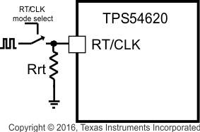 Figure 25. Works With Both RT Mode and CLK Mode
7.4.3 Bootstrap Voltage (BOOT) and Low-Dropout Operation
The device has an integrated boot regulator, and requires a small ceramic capacitor between the BOOT and PH pins to provide the gate drive voltage for the high-side MOSFET. The boot capacitor is charged when the BOOT pin voltage is less than VIN and BOOT-PH voltage is below regulation. The value of this ceramic capacitor should be 0.1 μF. A ceramic capacitor with an X7R or X5R grade dielectric with a voltage rating of 10 V or higher is recommended because of the stable characteristics over temperature and voltage.
To improve dropout, the device is designed to operate at 100% duty cycle as long as the BOOT to PH pin voltage is greater than the BOOT-PH UVLO threshold which is typically 2.1 V. When the voltage between BOOT and PH drops below the BOOT-PH UVLO threshold the high-side MOSFET is turned off and the low-side MOSFET is turned on allowing the boot capacitor to be recharged. In applications with split input voltage rails, 100% duty cycle operation can be achieved as long as (VIN – PVIN) > 4 V.
7.4.4 Sequencing (SS/TR)
Many of the common power supply sequencing methods can be implemented using the SS/TR, EN and PWRGD pins.
The sequential method is illustrated in Figure 26 using two TPS54620 devices. The power good of the first device is coupled to the EN pin of the second device which enables the second power supply when the primary supply reaches regulation. Figure 27 shows the results of Figure 26.
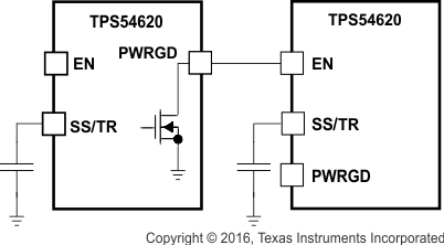 Figure 26. Sequential Start-Up Sequence
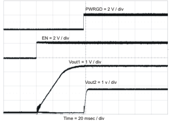 Figure 27. Sequential Start-Up Using EN and PWRGD
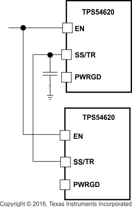
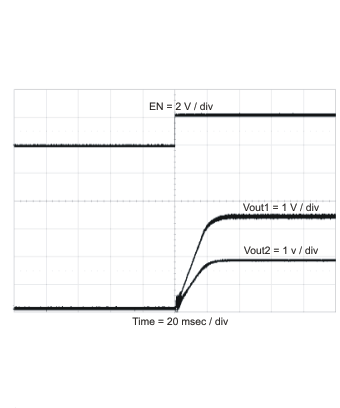
Figure 28 shows the method implementing ratiometric sequencing by connecting the SS/TR pins of two devices together. The regulator outputs ramp up and reach regulation at the same time. When calculating the slow start time the pullup current source must be doubled in Equation 4. Figure 29 shows the results of Figure 28.
Ratiometric and simultaneous power supply sequencing can be implemented by connecting the resistor network of R1 and R2 shown in Figure 30 to the output of the power supply that must be tracked or another voltage reference source. Using Equation 14 and Equation 15, the tracking resistors can be calculated to initiate the Vout2 slightly before, after or at the same time as Vout1. Equation 16 is the voltage difference between Vout1 and Vout2.
To design a ratiometric start-up in which the Vout2 voltage is slightly greater than the Vout1 voltage when Vout2 reaches regulation, use a negative number in Equation 14 and Equation 15 for ΔV. Equation 16 results in a positive number for applications where the Vout2 is slightly lower than Vout1 when Vout2 regulation is achieved. Figure 31 and Figure 32 show the results for positive ΔV and negative ΔV, respectively.
The ΔV variable is zero volt for simultaneous sequencing. To minimize the effect of the inherent SS/TR to VSENSE offset (Vssoffset, 29 mV) in the slow-start circuit and the offset created by the pullup current source (Iss, 2.3 μA) and tracking resistors, the Vssoffset and Iss are included as variables in the equations. Figure 33 shows the result when ΔV = 0 V.
To ensure proper operation of the device, the calculated R1 value from Equation 14 must be greater than the value calculated in Equation 17.


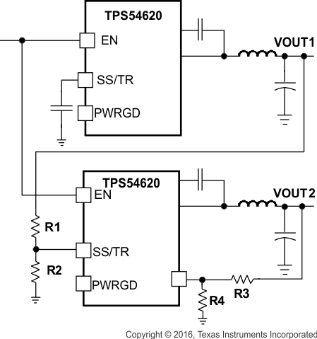 Figure 30. Ratiometric and Simultaneous Start-Up Sequence
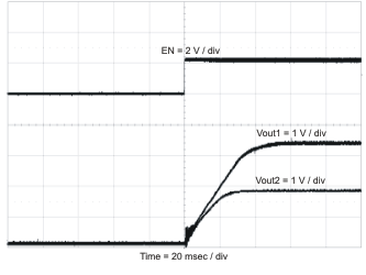 Figure 31. Ratiometric Start-Up With Vout1 Leading Vout2
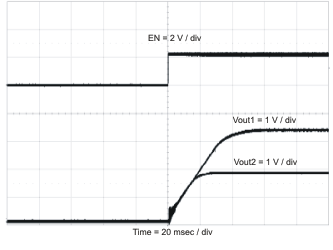 Figure 33. Simultaneous Start-Up
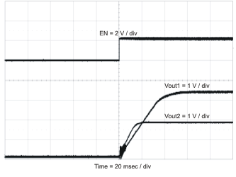 Figure 32. Ratiometric Start-Up With Vout2 Leading Vout1
