SLVS949F May 2009 – May 2017 TPS54620
PRODUCTION DATA.
- 1 Features
- 2 Applications
- 3 Description
- 4 Revision History
- 5 Pin Configurations and Functions
- 6 Specifications
-
7 Detailed Description
- 7.1 Overview
- 7.2 Functional Block Diagram
- 7.3
Feature Description
- 7.3.1 Fixed Frequency PWM Control
- 7.3.2 Continuous Current Mode Operation (CCM)
- 7.3.3 VIN and Power VIN Pins (VIN and PVIN)
- 7.3.4 Voltage Reference
- 7.3.5 Adjusting the Output Voltage
- 7.3.6 Safe Start-Up into Prebiased Outputs
- 7.3.7 Error Amplifier
- 7.3.8 Slope Compensation
- 7.3.9 Enable and Adjusting Undervoltage Lockout
- 7.3.10 Adjustable Switching Frequency and Synchronization (RT/CLK)
- 7.3.11 Slow Start (SS/TR)
- 7.3.12 Power Good (PWRGD)
- 7.3.13 Output Overvoltage Protection (OVP)
- 7.3.14 Overcurrent Protection
- 7.3.15 Thermal Shutdown
- 7.3.16 Small Signal Model for Loop Response
- 7.3.17 Simple Small Signal Model for Peak Current Mode Control
- 7.3.18 Small Signal Model for Frequency Compensation
- 7.4 Device Functional Modes
-
8 Application and Implementation
- 8.1 Application Information
- 8.2
Typical Application
- 8.2.1 Design Requirements
- 8.2.2
Detailed Design Procedures
- 8.2.2.1 Custom Design With WEBENCH Tools
- 8.2.2.2 Operating Frequency
- 8.2.2.3 Output Inductor Selection
- 8.2.2.4 Output Capacitor Selection
- 8.2.2.5 Input Capacitor Selection
- 8.2.2.6 Slow-Start Capacitor Selection
- 8.2.2.7 Bootstrap Capacitor Selection
- 8.2.2.8 Undervoltage Lockout Set Point
- 8.2.2.9 Output Voltage Feedback Resistor Selection
- 8.2.2.10 Compensation Component Selection
- 8.2.2.11 Fast Transient Considerations
- 8.2.3 Application Curves
- 9 Power Supply Recommendations
- 10Layout
- 11Device and Documentation Support
- 12Mechanical, Packaging, and Orderable Information
Package Options
Refer to the PDF data sheet for device specific package drawings
Mechanical Data (Package|Pins)
- RHL|14
- RGY|14
Thermal pad, mechanical data (Package|Pins)
Orderable Information
6 Specifications
6.1 Absolute Maximum Ratings(1)
(1) Stresses beyond those listed under Absolute Maximum Ratings may cause permanent damage to the device. These are stress ratings only, which do not imply functional operation of the device at these or any other conditions beyond those indicated under Recommended Operating Conditions. Exposure to absolute-maximum-rated conditions for extended periods may affect device reliability.
6.2 ESD Ratings
| VALUE | UNIT | |||
|---|---|---|---|---|
| V(ESD) | Electrostatic discharge | Human-body model (HBM), per ANSI/ESDA/JEDEC JS-001(1) | ±2000 | V |
| Charged-device model (CDM), per JEDEC specification JESD22-C101(2) | ±500 | |||
(1) JEDEC document JEP155 states that 500-V HBM allows safe manufacturing with a standard ESD control process.
(2) JEDEC document JEP157 states that 250-V CDM allows safe manufacturing with a standard ESD control process.
6.3 Recommended Operating Conditions
over operating free-air temperature range (unless otherwise noted)| MIN | NOM | MAX | UNIT | ||
|---|---|---|---|---|---|
| VIN | Input voltage | 4.5 | 17 | V | |
| PVIN | Power stage input voltage | 1.6 | 17 | V | |
| Output current | 0 | 6 | A | ||
| TJ | Operating junction temperature | –40 | 150 | °C | |
6.4 Thermal Information
| THERMAL METRIC(1) | TPS54620 | UNIT | ||
|---|---|---|---|---|
| RGY (VQFN) | RHL (VQFN) | |||
| 14 PINS | 14 PINS | |||
| RθJA | Junction-to-ambient thermal resistance | 40.1 | 40.1 | °C/W |
| RθJCtop | Junction-to-case (top) thermal resistance | 34.4 | 34.4 | °C/W |
| RθJB | Junction-to-board thermal resistance | 11.4 | 11.4 | °C/W |
| ψJT | Junction-to-top characterization parameter | 0.5 | 0.5 | °C/W |
| ψJB | Junction-to-board characterization parameter | 11.4 | 11.4 | °C/W |
| RθJCbot | Junction-to-case (bottom) thermal resistance | 1.8 | 1.8 | °C/W |
(1) For more information about traditional and new thermal metrics, see the Semiconductor and IC Package Thermal Metrics application report.
6.5 Electrical Characteristics
TJ = –40°C to 150°C, VIN = 4.5 V to 17 V, PVIN = 1.6 V to 17 V (unless otherwise noted)| PARAMETER | TEST CONDITIONS | MIN | TYP | MAX | UNIT |
|---|---|---|---|---|---|
| SUPPLY VOLTAGE (VIN AND PVIN PINS) | |||||
| PVIN operating input voltage | 1.6 | 17 | V | ||
| VIN operating input voltage | 4.5 | 17 | V | ||
| VIN internal UVLO threshold | VIN rising | 4 | 4.5 | V | |
| VIN internal UVLO hysteresis | 150 | mV | |||
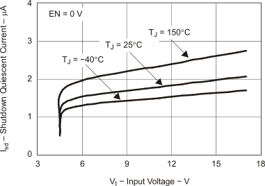
| VIN shutdown supply Current | EN = 0 V | 2 | 5 | μA | |
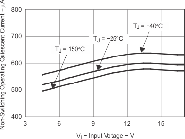
| VIN operating—nonswitching supply current | VSENSE = 810 mV | 600 | 800 | μA | |
| ENABLE AND UVLO (EN PIN) | |||||
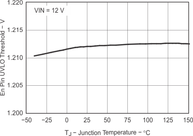
| Enable threshold | Rising | 1.21 | 1.26 | V | |
| Enable threshold | Falling | 1.10 | 1.17 | V | |
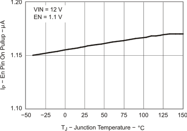
| Input current | EN = 1.1 V | 1.15 | μA | ||
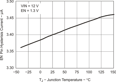
| Hysteresis current | EN = 1.3 V | 3.4 | μA | ||
| VOLTAGE REFERENCE | |||||
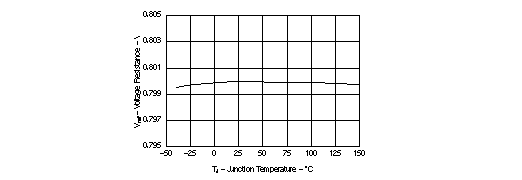
| Voltage reference | 0 A ≤ IOUT ≤ 6 A | 0.792 | 0.8 | 0.808 | V |
| MOSFET | |||||
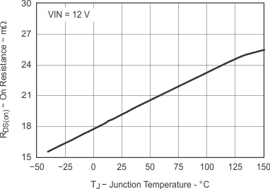
| High-side switch resistance | BOOT-PH = 3 V | 32 | 60 | mΩ | |
| High-side switch resistance(1) | BOOT-PH = 6 V | 26 | 40 | mΩ | |
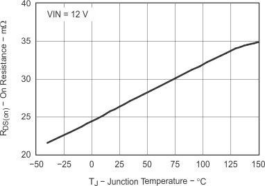
| Low-side Switch Resistance(1) | VIN = 12 V | 19 | 30 | mΩ | |
| ERROR AMPLIFIER | |||||
| Error amplifier Transconductance (gm) | –2 μA < ICOMP < 2 μA, V(COMP) = 1 V | 1300 | μMhos | ||
| Error amplifier DC gain | VSENSE = 0.8 V | 1000 | 3100 | V/V | |
| Error amplifier source/sink | V(COMP) = 1 V, 100-mV input overdrive | ±110 | μA | ||
| Start switching threshold | 0.25 | V | |||
| COMP to Iswitch gm | 16 | A/V | |||
| CURRENT LIMIT | |||||
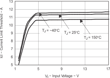
| High-side switch current limit threshold | 8 | 11 | A | ||
| Low-side switch sourcing current limit | 7 | 10 | A | ||
| Low-side switch sinking current limit | 2.3 | A | |||
| THERMAL SHUTDOWN | |||||
| Thermal shutdown | 160 | 175 | °C | ||
| Thermal shutdown hysteresis | 10 | °C | |||
| TIMING RESISTOR AND EXTERNAL CLOCK (RT/CLK PIN) | |||||
| Minimum switching frequency | Rrt = 240 kΩ (1%) | 160 | 200 | 240 | kHz |
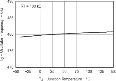
| Switching frequency | Rrt = 100 kΩ (1%) | 400 | 480 | 560 | kHz |
| Maximum switching frequency | Rrt = 29 kΩ (1%) | 1440 | 1600 | 1760 | kHz |
| Minimum pulse width | 20 | ns | |||
| RT/CLK high threshold | 2 | V | |||
| RT/CLK low threshold | 0.8 | V | |||
| RT/CLK falling edge to PH rising edge delay | Measured at 500 kHz with RT resistor in series | 66 | ns | ||
| Switching frequency range (RT mode set point and PLL mode) | 200 | 1600 | kHz | ||
| PH (PH PIN) | |||||
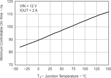
| Minimum on-time | Measured at 90% to 90% of VIN, 25°C, IPH = 2 A | 94 | 135 | ns | |
| Minimum off-time | BOOT-PH ≥ 3 V | 0 | ns | ||
| BOOT (BOOT PIN) | |||||
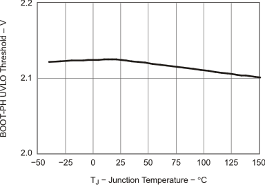
| BOOT-PH UVLO | 2.1 | 3 | V | ||
| SLOW START AND TRACKING (SS/TR PIN) | |||||
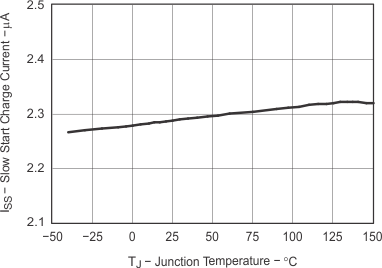
| SS charge current | 2.3 | μA | |||
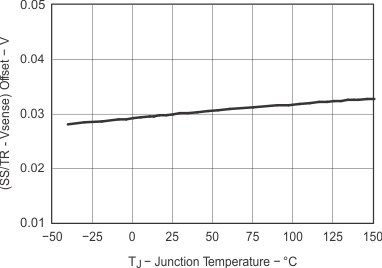
| SS/TR to VSENSE matching | V(SS/TR) = 0.4 V | 29 | 60 | mV | |
| POWER GOOD (PWRGD PIN) | |||||
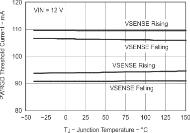
| VSENSE threshold | VSENSE falling (Fault) | 91 | % Vref | ||
| VSENSE rising (Good) | 94 | % Vref | |||
| VSENSE rising (Fault) | 109 | % Vref | |||
| VSENSE falling (Good) | 106 | % Vref | |||
| Output high leakage | VSENSE = Vref, V(PWRGD) = 5.5 V | 30 | 100 | nA | |
| Output low | I(PWRGD) = 2 mA | 0.3 | V | ||
| Minimum VIN for valid output | V(PWRGD) < 0.5 V at 100 μA | 0.6 | 1 | V | |
| Minimum SS/TR voltage for PWRGD | 1.4 | V | |||
(1) Measured at pins
6.6 Typical Characteristics
