SLVSEW1B April 2019 – April 2019 TPS566235
PRODUCTION DATA.
- 1 Features
- 2 Applications
- 3 Description
- 4 Revision History
- 5 Pin Configuration and Functions
- 6 Specifications
- 7 Detailed Description
- 8 Application and Implementation
- 9 Power Supply Recommendations
- 10Layout
- 11Device and Documentation Support
- 12Mechanical, Packaging, and Orderable Information
Package Options
Mechanical Data (Package|Pins)
- RJN|13
Thermal pad, mechanical data (Package|Pins)
Orderable Information
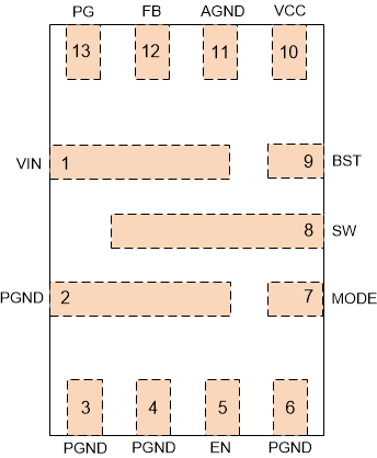
5 Pin Configuration and Functions
RJN Package
13-Pin VQFN
Top View

Pin Functions
| PIN | I/O | DESCRIPTION | |
|---|---|---|---|
| NAME | NO. | ||
| VIN | 1 | P | Input voltage supply pin for the control circuitry. Connect the input decoupling capacitors between VIN and PGND. |
| PGND | 2,3,4,6 | G | Power GND terminal for the controller circuit and the internal circuitry. |
| EN | 5 | I | Enable pin of Buck converter. EN pin is a digital input pin, decides turn on/off Buck converter. Internal pull down current to disable converter if leave this pin open. |
| MODE | 7 | I | Eco-Mode™/OOA/FCCM Mode selection pin with external 1% resistor or connecting to VCC. |
| SW | 8 | O | Switching node connection to the output inductor and bootstrap capacitor. |
| BST | 9 | I | Supply input for the gate drive voltage of the high-side MOSFET. Connect the bootstrap capacitor between BST and SW, 0.1 uF is recommended. |
| VCC | 10 | P | Internal LDO output for control and driver. Decouple with a minimum 1 μF ceramic capacitor as close to VCC as possible. |
| AGND | 11 | G | Ground of internal analog circuitry. Connect AGND to GND plane with a short trace. |
| FB | 12 | I | Feedback sensing pin for Buck output voltage. Connect this pin to the resistor divider between output voltage and AGND. |
| PG | 13 | O | Open drain power good indicator. It is asserted low if output voltage is out of PG threshold, over voltage or if the device is under thermal shutdown, EN shutdown or during soft start. |