SLVSEG1A July   2018  – September 2019 TPS56637

PRODUCTION DATA.  

  1. Features
  2. Applications
  3. Description
    1.     Device Images
      1.      Simplified Schematic
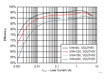
      2.      Efficiency vs Output Current VOUT = 5 V
  4. Revision History
  5. Pin Configuration and Functions
    1.     Pin Functions
  6. Specifications
    1. 6.1 Absolute Maximum Ratings
    2. 6.2 Handling Ratings
    3. 6.3 Recommended Operating Conditions
    4. 6.4 Thermal Information
    5. 6.5 Electrical Characteristics
    6. 6.6 Timing Requirements
    7. 6.7 Typical Characteristics
  7. Detailed Description
    1. 7.1 Overview
    2. 7.2 Functional Block Diagram
    3. 7.3 Feature Description
      1. 7.3.1  The Adaptive On-Time Control and PWM Operation
      2. 7.3.2  Mode Selection
        1. 7.3.2.1 Eco-mode™ Control Scheme
        2. 7.3.2.2 FCCM Control
      3. 7.3.3  Soft Start and Pre-Biased Soft Start
      4. 7.3.4  Enable and Adjusting Undervoltage Lockout
      5. 7.3.5  Output Overcurrent Limit and Undervoltage Protection
      6. 7.3.6  Overvoltage Protection
      7. 7.3.7  UVLO Protection
      8. 7.3.8  Thermal Shutdown
      9. 7.3.9  Output Voltage Discharge
      10. 7.3.10 Power Good
    4. 7.4 Device Functional Modes
      1. 7.4.1 Standby Operation
      2. 7.4.2 Normal Operation
      3. 7.4.3 Light Load Operation
  8. Application and Implementation
    1. 8.1 Application Information
    2. 8.2 Typical Application
      1. 8.2.1 Design Requirements
      2. 8.2.2 Detailed Design Procedure
        1. 8.2.2.1 Output Voltage Resistors Selection
        2. 8.2.2.2 Output Filter Selection
        3. 8.2.2.3 Input Capacitor Selection
        4. 8.2.2.4 Bootstrap Capacitor Selection
      3. 8.2.3 Application Curves
  9. Power Supply Recommendations
  10. 10Layout
    1. 10.1 Layout Guidelines
    2. 10.2 Layout Example
  11. 11Device and Documentation Support
    1. 11.1 Documentation Support
      1. 11.1.1 Related Documentation
    2. 11.2 Receiving Notification of Documentation Updates
    3. 11.3 Community Resources
    4. 11.4 Trademarks
    5. 11.5 Electrostatic Discharge Caution
    6. 11.6 Glossary
  12. 12Mechanical, Packaging, and Orderable Information
    1. 12.1 Package Option Addendum
      1. 12.1.1 Packaging Information
      2. 12.1.2 Tape and Reel Information

Package Options

Mechanical Data (Package|Pins)
Thermal pad, mechanical data (Package|Pins)
Orderable Information

Application Curves

TPS56637 5VoutAppEfficiency2P1.gif
Figure 18. Efficiency
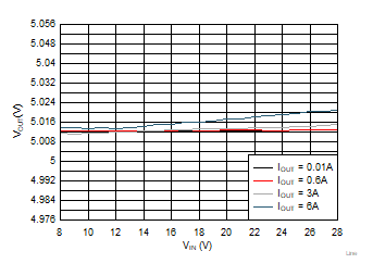
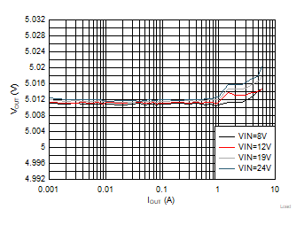
TPS56637 LineRegulation2P1.gif
Figure 20. Line Regulation
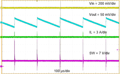
TPS56637 0A01Ripple-slvseg1.gif
Figure 22. Steady State Waveforms, IOUT = 0.01 A
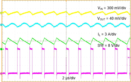
TPS56637 3ARipple-slvseg1.gif
Figure 24. Steady State Waveforms, IOUT= 3 A
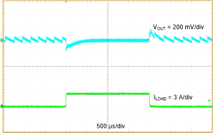
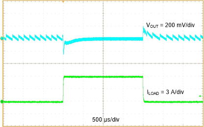
TPS56637 0A-3ALoadTrans-slvseg1.gif
Figure 26. Transient Response 0 to 3 A
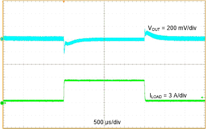
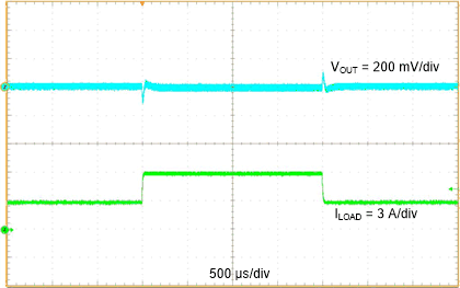
TPS56637 0A6-5A4LoadTrans-slvseg1.gif
Figure 28. Transient Response 0.6 to 5.4 A
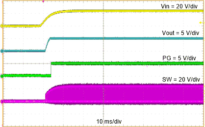
TPS56637 VINStartup-slvseg1.gif
Figure 30. Startup Relative to VIN
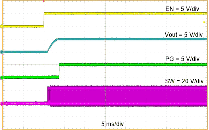
TPS56637 ENStartup-slvseg1.gif
Figure 32. Enable Relative to EN
TPS56637 Loadregulation2P1.gif
Figure 19. Load Regulation
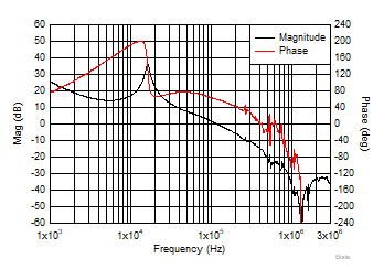
TPS56637 Bode-plot2p0-slvseg1.gif
VIN = 24V VOUT = 5V IOUT = 6A
Figure 21. Bode Plot
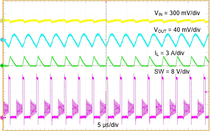
TPS56637 0A6Ripple-slvseg1.gif
Figure 23. Steady State Waveforms, IOUT= 0.6 A
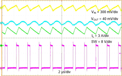
TPS56637 6ARipple-slvseg1.gif
Figure 25. Steady State Waveforms, IOUT= 6 A
TPS56637 0A-6ALoadTrans-slvseg1.gif
Figure 27. Transient Response 0 to 6 A
TPS56637 3A-6ALoadTrans-slvseg1.gif
Figure 29. Transient Response 3 to 6 A
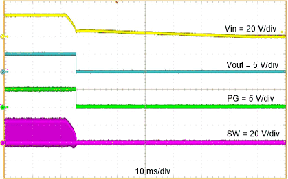
TPS56637 VINShutdown-slvseg1.gif
Figure 31. Shutdown Relative to VIN
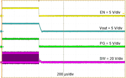
TPS56637 ENShutdown-slvseg1.gif
Figure 33. Disable Relative to EN