SLVSEG1A July   2018  – September 2019 TPS56637

PRODUCTION DATA.  

  1. Features
  2. Applications
  3. Description
    1.     Device Images
      1.      Simplified Schematic
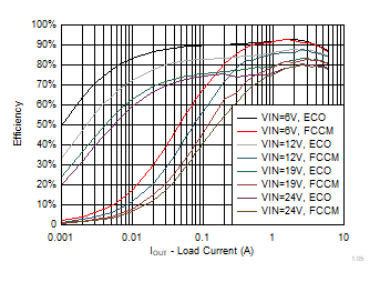
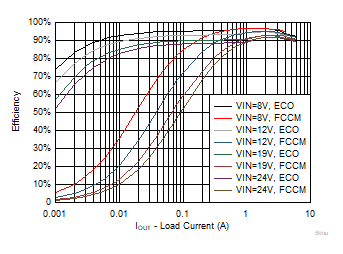
      2.      Efficiency vs Output Current VOUT = 5 V
  4. Revision History
  5. Pin Configuration and Functions
    1.     Pin Functions
  6. Specifications
    1. 6.1 Absolute Maximum Ratings
    2. 6.2 Handling Ratings
    3. 6.3 Recommended Operating Conditions
    4. 6.4 Thermal Information
    5. 6.5 Electrical Characteristics
    6. 6.6 Timing Requirements
    7. 6.7 Typical Characteristics
  7. Detailed Description
    1. 7.1 Overview
    2. 7.2 Functional Block Diagram
    3. 7.3 Feature Description
      1. 7.3.1  The Adaptive On-Time Control and PWM Operation
      2. 7.3.2  Mode Selection
        1. 7.3.2.1 Eco-mode™ Control Scheme
        2. 7.3.2.2 FCCM Control
      3. 7.3.3  Soft Start and Pre-Biased Soft Start
      4. 7.3.4  Enable and Adjusting Undervoltage Lockout
      5. 7.3.5  Output Overcurrent Limit and Undervoltage Protection
      6. 7.3.6  Overvoltage Protection
      7. 7.3.7  UVLO Protection
      8. 7.3.8  Thermal Shutdown
      9. 7.3.9  Output Voltage Discharge
      10. 7.3.10 Power Good
    4. 7.4 Device Functional Modes
      1. 7.4.1 Standby Operation
      2. 7.4.2 Normal Operation
      3. 7.4.3 Light Load Operation
  8. Application and Implementation
    1. 8.1 Application Information
    2. 8.2 Typical Application
      1. 8.2.1 Design Requirements
      2. 8.2.2 Detailed Design Procedure
        1. 8.2.2.1 Output Voltage Resistors Selection
        2. 8.2.2.2 Output Filter Selection
        3. 8.2.2.3 Input Capacitor Selection
        4. 8.2.2.4 Bootstrap Capacitor Selection
      3. 8.2.3 Application Curves
  9. Power Supply Recommendations
  10. 10Layout
    1. 10.1 Layout Guidelines
    2. 10.2 Layout Example
  11. 11Device and Documentation Support
    1. 11.1 Documentation Support
      1. 11.1.1 Related Documentation
    2. 11.2 Receiving Notification of Documentation Updates
    3. 11.3 Community Resources
    4. 11.4 Trademarks
    5. 11.5 Electrostatic Discharge Caution
    6. 11.6 Glossary
  12. 12Mechanical, Packaging, and Orderable Information
    1. 12.1 Package Option Addendum
      1. 12.1.1 Packaging Information
      2. 12.1.2 Tape and Reel Information

Package Options

Mechanical Data (Package|Pins)
Thermal pad, mechanical data (Package|Pins)
Orderable Information

Typical Characteristics

VIN = 12 V (unless otherwise noted)
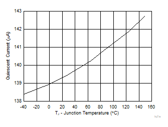
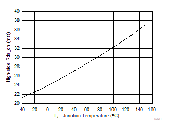
TPS56637 IqTemp2p1.gif
Figure 1. Quiescent Current vs Temperature
TPS56637 RdsHSF.gif
Figure 3. High-Side RDS(on) vs Temperature
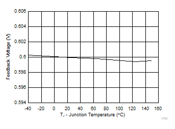
TPS56637 Vfb2p1.gif
Figure 5. Feedback Voltage vs Temperature
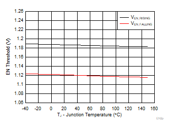
TPS56637 EN2p1.gif
Figure 7. EN Threshold vs Temperature
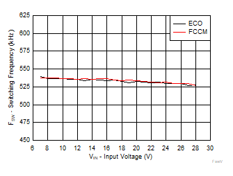
TPS56637 FswVin2p1.gif
VOUT=5 V IOUT = 6 A
Figure 9. Switching Frequency vs Input voltage
TPS56637 1pt05VoutEfficiency2P1.gif
Figure 11. VOUT = 1.05 V Efficiency, L = 1 µH
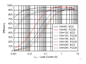
TPS56637 5VoutEfficiency2P1.gif
Figure 13. VOUT = 5 V Efficiency, L = 3.3 µH
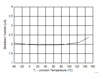
TPS56637 IsdTemp2p1.gif
Figure 2. Shutdown Current vs Temperature
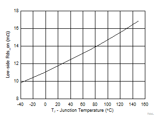
TPS56637 RdsLSF.gif
Figure 4. Low-side RDS(on) vs Temperature
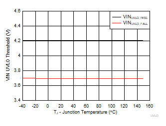
TPS56637 UVLO2p1.gif
Figure 6. VIN UVLO Threshold vs Temperature
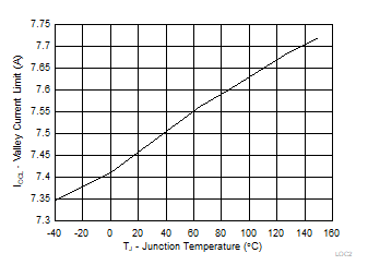
TPS56637 LOC2p1.gif
Figure 8. Valley Current Limit vs Temperature
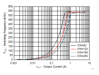
TPS56637 FswLoadingECO2p1.gif
VOUT = 5 V L = 3.3 µH Eco-mode™
Figure 10. Switching Frequency vs Output Current
TPS56637 3pt3VoutEfficiency2P1.gif
Figure 12. VOUT = 3.3 V Efficiency, L = 2.2 µH
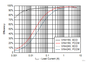
TPS56637 12VoutEfficiency2P1.gif
Figure 14. VOUT = 12 V Efficiency, L = 5.6 µH