SLVSE52A September 2018 – November 2018 TPS61088-Q1
PRODUCTION DATA.
- 1 Features
- 2 Applications
- 3 Description
- 4 Revision History
- 5 Description (continued)
- 6 Pin Configuration and Functions
- 7 Specifications
- 8 Detailed Description
- 9 Application and Implementation
- 10Power Supply Recommendations
- 11Layout
- 12Device and Documentation Support
- 13Mechanical, Packaging, and Orderable Information
Package Options
Mechanical Data (Package|Pins)
- RHL|20
Thermal pad, mechanical data (Package|Pins)
- RHL|20
Orderable Information
8.4.1.2 PFM Mode
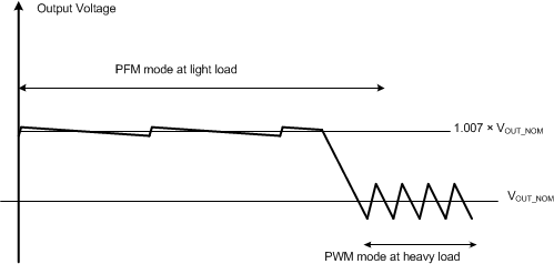
The TPS61088-Q1 improves the efficiency at light load with the PFM mode. When the converter operates in light load condition, the output of the internal error amplifier decreases to make the inductor peak current down, delivering less power to the load. When the output current further reduces, the current through the inductor will decrease to zero during the off-time. Once the current through the high side N-MOSFET is zero, the high-side MOSFET is turned off until the beginning of the next switching cycle. When the output of the error amplifier continuously goes down and reaches a threshold with respect to the peak current of ILIM / 12, the output of the error amplifier is clamped at this value and does not decrease any more. If the load current is smaller than what the TPS61088-Q1 delivers, the output voltage increases above the nominal setting output voltage. The TPS61088-Q1 extends its off time of the switching period to deliver less energy to the output and regulate the output voltage to 0.7% higher than the nominal setting voltage. With the PFM operation mode, the TPS61088-Q1 keeps the efficiency above 80% even when the load current decreases to 1 mA. In addition, the output voltage ripple is much smaller at light load due to low peak current. Refer to Figure 12.
 Figure 12. PFM Mode Diagram