SLVSCO6 January 2015 TPS61093-Q1
PRODUCTION DATA.
- 1 Features
- 2 Applications
- 3 Description
- 4 Simplified Schematic
- 5 Revision History
- 6 Pin Configuration and Functions
- 7 Specifications
- 8 Detailed Description
- 9 Application and Implementation
- 10Power Supply Recommendations
- 11Layout
- 12Device and Documentation Support
- 13Mechanical, Packaging, and Orderable Information
Package Options
Mechanical Data (Package|Pins)
- DSK|10
Thermal pad, mechanical data (Package|Pins)
- DSK|10
Orderable Information
8 Detailed Description
8.1 Overview
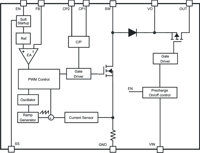
The TPS61093-Q1 is a highly integrated boost regulator for up to 17-V output. In addition to the on-chip 1-A PWM switch and power diode, this IC also integrates an output-side isolation switch as shown in the functional block diagram. One common issue with conventional boost regulators is the conduction path from input to output even when the PWM switch is turned off. It creates three problems, which are inrush current during start-up, output leakage current during shutdown, and excessive over load current. In the TPS61093-Q1, the isolation switch turns off under shutdown-mode and over load conditions, thereby opening the current path. However, shorting the VO and OUT pins bypasses the isolation switch and enhances efficiency. Because the isolation switch is on the output side, the IC's VIN pin and power stage input power (up to 10 V) can be separated.
The TPS61093-Q1 adopts current-mode control with constant pulse-width-modulation (PWM) frequency. The switching frequency is fixed at 1.2-MHz typical. PWM operation turns on the PWM switch at the beginning of each switching cycle. The input voltage is applied across the inductor and the inductor current ramps up. In this mode, the output capacitor is discharged by the load current. When the inductor current hits the threshold set by the error amplifier output, the PWM switch is turned off, and the power diode is forward-biased. The inductor transfers its stored energy to replenish the output capacitor. This operation repeats in the next switching cycle. The error amplifier compares the FB-pin voltage with an internal reference, and its output determines the duty cycle of the PWM switching. This closed-loop system requires frequency compensation for stable operation. The device has a built-in compensation circuit that can accommodate a wide range of input and output voltages. To avoid the sub-harmonic oscillation intrinsic to current-mode control, the IC also integrates slope compensation, which adds an artificial slope to the current ramp.
8.2 Functional Block Diagram

8.3 Feature Description
8.3.1 Shutdown And Load Discharge
When the EN pin is pulled low for 1-ms, the IC stops the PWM switch and turns off the isolation switch, providing isolation between input and output. The internal current path consisting of the isolation switch’s body diode and several parasitic diodes quickly discharges the output voltage to less than 3.3-V. Afterwards, the voltage is slowly discharged to zero by the leakage current. This protects the IC and the external components from high voltage in shutdown mode.
In shutdown mode, less than 5-μA of input current is consumed by the IC.
8.3.2 Over Load And Over Voltage Protection
If the over load current passing through the isolation switch is above the over load limit (IOL) for 3-μs (typ), the TPS61093-Q1 is switched off until the fault is cleared and the EN pin toggles. The function only is triggered 52-ms after the IC is enabled.
To prevent the PWM switch and the output capacitor from exceeding maximum voltage ratings, an over voltage protection circuit turns off the boost switch as soon as the output voltage at the VO pin exceeds the OVP threshold. Simultaneously, the IC opens the isolation switch. The regulator resumes PWM switching after the VO pin voltage falls 0.6-V below the threshold.
8.3.3 Under Voltage Lockout (UVLO)
An under voltage lockout prevents improper operation of the device for input voltages below 1.55-V. When the input voltage is below the under voltage threshold, the entire device, including the PWM and isolation switches, remains off.
8.3.4 Thermal Shutdown
An internal thermal shutdown turns off the isolation and PWM switches when the typical junction temperature of 150°C is exceeded. The thermal shutdown has a hysteresis of 15°C, typical.
8.4 Device Functional Modes
The converter operates in continuous conduction mode (CCM) as soon as the input current increases above half the ripple current in the inductor, for lower load currents it switches into discontinuous conduction mode (DCM). If the load is further reduced, the part starts to skip pulses to maintain the output voltage.