SLVS625E February 2006 – November 2015 TPS61150 , TPS61151
PRODUCTION DATA.
- 1 Features
- 2 Applications
- 3 Description
- 4 Revision History
- 5 Device Comparison Tables
- 6 Pin Configuration and Functions
- 7 Specifications
- 8 Detailed Description
- 9 Application and Implementation
- 10Power Supply Recommendations
- 11Layout
- 12Device and Documentation Support
- 13Mechanical, Packaging, and Orderable Information
Package Options
Mechanical Data (Package|Pins)
- DRC|10
Thermal pad, mechanical data (Package|Pins)
- DRC|10
Orderable Information
8 Detailed Description
8.1 Overview
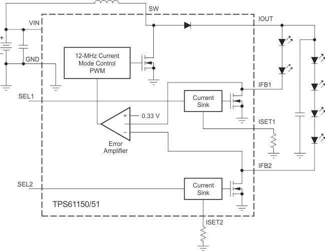
The TPS6115x is a two-channel WLED driver with an integrated inductive boost converter. The boost converter generates the bias voltage for the LED string while the two integrated low-side current sinks independently regulate the current in LED strings from VIN to 29 V. Independent LED string dimming is provided via a PWM input at the SEL1 and SEL2 inputs.
8.2 Functional Block Diagram

8.3 Feature Description
8.3.1 Start-Up
During start-up, both the boost converter and the current sink circuitry ramp up simultaneously to establish a steady state. The current sink circuitry ramps up current in 16 steps with each step taking 64 clock cycles. This period ensures that the current sink loop is slower than the boost converter response during start-up. Therefore, the boost converter output comes up slowly as current sink circuitry ramps up the current. This configuration ensures a smooth start-up and minimizes in-rush current.
8.3.2 Overvoltage Protection (OVP)
To prevent the boost output runaway as the result of WLED disconnection, there is an overvoltage protection circuit that stops the boost converter from switching as soon as its output exceeds the OVP threshold. When the voltage falls below the OVP threshold, the converter resumes switching.
The two OVP options offer the choices to prevent a 25-V rated output capacitor or the internal 30-V FET from breaking down.
8.3.3 Undervoltage Lockout
An undervoltage lockout prevents device malfunction at input voltages below 1.65 V (typical). When the input voltage is below the undervoltage threshold, the device remains off, and both the boost converter and current sink circuit are turned off, providing isolation between input and output.
8.3.4 Thermal Shutdown
An internal thermal shutdown turns off the device when the typical junction temperature of 160°C is exceeded. The thermal shutdown has a hysteresis of typically 15°C.
8.3.5 Enable
Pulling either the SEL1 or SEL2 pin low turns off the corresponding output. If both SEL1 and SEL2 are low for more than 40 ms, the device shuts down and consumes less than 1 μA current. The SEL pin can also be used for PWM brightness dimming. To improve PWM dimming linearity, soft start is disabled if the time from the falling and rising edges of two adjacent SELx pulses is less than 40 ms. See the Application and Implementation section for details.
Each SEL input pin has an internal pulldown resistor to disable the device when the pin is floating.
8.4 Device Functional Modes
8.4.1 Current Regulation
The TPS6115x uses a single boost regulator to drive two WLED strings, each with independently programmable current. The boost converter adopts PWM control which is ideal for high output current and low output ripple noises. The feedback loop regulates the IFB pins to a threshold voltage (330 mV typical), giving the current sink circuit just enough headroom to operate.
The regulation current is set by the resistor on the ISET pin based on Equation 1.

where
- IO = output current
- VISET = ISET pin voltage (1.229 V typical)
- RSET = ISET pin resistor value
- KISET = current multiplier (900 typical)
When both outputs are enabled, the boost converter provides enough power to provide the demanded current through IFB1 and IFB2 while keeping the voltage at IOUT high enough to meet the forward voltage drops of the WLEDs. Specifically, at start-up, the boost converter increases its output power, and therefore the output voltage, from IOUT until IFB1 reaches its regulated voltage. Once IFB1 is within regulation, the device looks to the IFB2 voltage and may increase V(IOUT) further to get IFB2 in regulation. After both IFB pins reach regulation, the feedback path dynamically switches to whichever IFB pin drops more than the IFB low hysteresis voltage (60 mV typical) below its regulation voltage. This architecture ensures proper current regulation for both IFB1 pins; however, the voltage at one IFB pin is higher than the minimum required regulation voltage. The overall efficiency when both strings are on depends on the voltage difference between the IFB1 and IFB2 pins. A large difference reduces the efficiency as a result of power losses across the current sink circuit of the IFB pin with the higher drop.