SLVS625E February 2006 – November 2015 TPS61150 , TPS61151
PRODUCTION DATA.
- 1 Features
- 2 Applications
- 3 Description
- 4 Revision History
- 5 Device Comparison Tables
- 6 Pin Configuration and Functions
- 7 Specifications
- 8 Detailed Description
- 9 Application and Implementation
- 10Power Supply Recommendations
- 11Layout
- 12Device and Documentation Support
- 13Mechanical, Packaging, and Orderable Information
Package Options
Mechanical Data (Package|Pins)
- DRC|10
Thermal pad, mechanical data (Package|Pins)
- DRC|10
Orderable Information
7 Specifications
7.1 Absolute Maximum Ratings
over operating free-air temperature range (unless otherwise noted)(1)(2)| MIN | MAX | UNIT | ||
|---|---|---|---|---|
| Supply voltages on pin VIN(2) | –0.3 | V | ||
| Voltages on pins SEL1, SEL2, ISET1 and ISET2(2) | –0.3 | V | ||
| Voltage on pin IOUT, SW, IFB1 and IFB2(2) | 30 | V | ||
| Operating junction temperature | –40 | 150 | °C | |
| Storage temperature, Tstg | –65 | 150 | °C | |
(1) Stresses beyond those listed under Absolute Maximum Ratings may cause permanent damage to the device. These are stress ratings only, which do not imply functional operation of the device at these or any other conditions beyond those indicated under Recommended Operating Conditions. Exposure to absolute-maximum-rated conditions for extended periods may affect device reliability.
7.2 ESD Ratings
| VALUE | UNIT | |||
|---|---|---|---|---|
| V(ESD) | Electrostatic discharge | Human-body model (HBM), per ANSI/ESDA/JEDEC JS-001(1) | ±2000 | V |
| Charged-device model (CDM), per JEDEC specification JESD22-C101(2) | ±1500 | |||
(1) JEDEC document JEP155 states that 500-V HBM allows safe manufacturing with a standard ESD control process.
(2) JEDEC document JEP157 states that 250-V CDM allows safe manufacturing with a standard ESD control process.
7.3 Recommended Operating Conditions
over operating free-air temperature range (unless otherwise noted).| MIN | NOM | MAX | UNIT | ||
|---|---|---|---|---|---|
| VI | Input voltage | 2.5 | 6 | V | |
| VO | Output voltage | VIN | 27 | V | |
| L | Inductor(1) | 10 | μH | ||
| CIN | Input capacitor(1) | 1 | μF | ||
| CO | Output capacitor(1) | 1 | μF | ||
| TA | Operating ambient temperature | –40 | 85 | °C | |
| TJ | Operating junction temperature | –40 | 125 | °C | |
(1) See the Application and Implementation section for further information.
7.4 Thermal Information
| THERMAL METRIC(1) | TPS6115x | UNIT | |
|---|---|---|---|
| DRC (VSON) | |||
| 10 PINS | |||
| RθJA | Junction-to-ambient thermal resistance | 44.3 | °C/W |
| RθJC(top) | Junction-to-case (top) thermal resistance | 56.1 | °C/W |
| RθJB | Junction-to-board thermal resistance | 19.2 | °C/W |
| ψJT | Junction-to-top characterization parameter | 0.7 | °C/W |
| ψJB | Junction-to-board characterization parameter | 19.4 | °C/W |
| RθJC(bot) | Junction-to-case (bottom) thermal resistance | 5.5 | °C/W |
(1) For more information about traditional and new thermal metrics, see the Semiconductor and IC Package Thermal Metrics application report, SPRA953.
7.5 Electrical Characteristics
At VI = 3.6 V, SELx = VIN, RSET = 80 kΩ, VIO = 15 V, and TA = –40°C to +85°C. Typical values are at TA = 25°C (unless otherwise noted).| PARAMETER | TEST CONDITIONS | MIN | TYP | MAX | UNIT | |
|---|---|---|---|---|---|---|
| SUPPLY CURRENT | ||||||
| VI | Input voltage range | 2.5 | 6 | V | ||
| IQ | Operating quiescent current into VIN | Device PWM switching no load | 2 | mA | ||
| ISD | Shutdown current | SELx = GND | 1.5 | μA | ||
| VUVLO | Undervoltage lockout threshold | VIN falling | 1.65 | 1.8 | V | |
| Vhys | Undervoltage lockout hysterisis | 70 | mV | |||
| ENABLE AND SOFT START | ||||||
| V(selh) | SEL logic high voltage | VIN = 2.7 V to 6 V | 1.2 | V | ||
| V(sell) | SEL logic low voltage | VIN = 2.7 V to 6 V | 0.4 | V | ||
| R(en) | SEL pulldown resistor | 300 | 700 | kΩ | ||
| Toff | SEL pulse width to disable | SELx high to low | 40 | ms | ||
| Kss | IFB soft start current steps | 16 | ||||
| Tss | Soft start time step | Measured as clock divider | 64 | |||
| Tss_en | Soft start enable time | Time between falling and rising of two adjacent SELx pulses | 40 | ms | ||
| CURRENT FEEDBACK | ||||||
| V(ISET) | ISET pin voltage | 1.204 | 1.229 | 1.254 | V | |
| K(ISET) | Current multiplier | IOUT/ISET | 820 | 900 | 990 | |
| KM | Current matching | In reference to the average of two output current | –6% | 6% | ||
| V(IFB) | IFB regulation voltage | 300 | 330 | 360 | mV | |
| V(IFB_L) | IFB low threshold hysteresis | 60 | mV | |||
| Tisink | Current sink settle time measured from SELx rising edge(1) | 6 | μs | |||
| Ilkg | IFB pin leakage current | IFB voltage = 25 V | 1 | μA | ||
| POWER SWITCH AND DIODE | ||||||
| rDS(on) | N-channel MOSFET on-resistance | VIN = VGS = 3.6 V | 0.6 | 0.9 | Ω | |
| I(LN_NFET) | N-channel leakage current | VDS = 25 V | 1 | μA | ||
| VF | Power diode forward voltage | ID = 0.7 A | 0.83 | 1 | V | |
| OC AND OVP | ||||||
| ILIM | N-Channel MOSFET current limit | Dual output, IOUT = 15 V, D = 76% | 0.75 | 1 | 1.25 | A |
| Single output , IOUT = 15 V, D = 76% | 0.40 | 0.55 | 0.7 | |||
| I(IFB_MAX) | Current sink max output current | IFB = 330 mV | 35 | mA | ||
| VOVP | Overvoltage threshold | TPS61150 | 27 | 28 | 29 | V |
| TPS61151 | 21 | 22 | 23 | |||
| VOVP(hys) | Overvoltage hysteresis | TPS61150 | 550 | mV | ||
| TPS61151 | 440 | |||||
| PWM AND PFM CONTROL | ||||||
| ƒS | Oscillator frequency | 1 | 1.2 | 1.5 | MHz | |
| Dmax | Maximum duty cycle | VFB = 1 V | 90% | 93% | ||
| THERMAL SHUTDOWN | ||||||
| Tshutdown | Thermal shutdown threshold | 160 | °C | |||
| Thys | Thermal shutdown threshold hysteresis | 15 | °C | |||
7.6 Typical Characteristics
Data for all characteristic graphs were taken using the Typical Application with inductor = 10 μH (VLCF4018T-100MR74-2), R1 = R2 = 56 kΩ, unless otherwise noted.Table 3. Table Of Graphs
| FIGURE | ||
|---|---|---|
| Overcurrent limit | VIN = 3 V, 3.6 V, and 4 V, Single and dual output | Figure 1, Figure 2 |
| K value over current | VIN = 3.6 V, ILOAD = 2 mA to 25 mA | Figure 3 |
| PWM dimming linearity | Frequency = 20 kHz and 30 kHz | Figure 4 |
| Single output PWM dimming waveform | Figure 5 | |
| Multiplexed PWM dimming waveform | Figure 6 | |
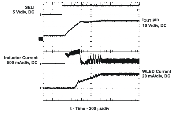
| Start-up waveform | Figure 7 | |
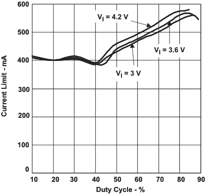 Figure 1. Overcurrent Limit (Single Output) vs Duty Cycle
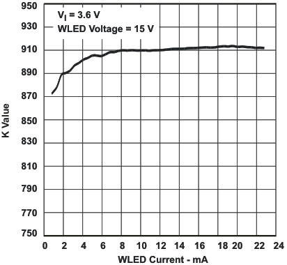 Figure 3. K Value vs WLED Current
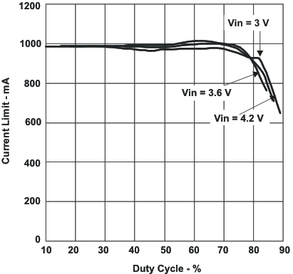 Figure 2. Overcurrent Limit (Dual Output) vs Duty Cycle
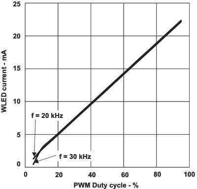 Figure 4. WLED Brightness Dimming Linearity
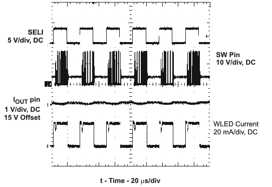 Figure 5. Single Output WLED PWM Brightness Dimming
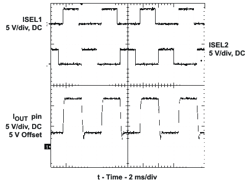
| ISEL1: 4 WLED | ISEL2: 2 WLED |