SLVSB73B December 2011 – May 2015 TPS61165-Q1
PRODUCTION DATA.
- 1 Features
- 2 Applications
- 3 Description
- 4 Revision History
- 5 Pin Configuration and Functions
- 6 Specifications
- 7 Detailed Description
- 8 Application and Implementation
- 9 Power Supply Recommendations
- 10Layout
- 11Device and Documentation Support
- 12Mechanical, Packaging, and Orderable Information
Package Options
Mechanical Data (Package|Pins)
- DBV|6
Thermal pad, mechanical data (Package|Pins)
Orderable Information
1 Features
- Qualified for Automotive Applications
- 40-V Maximum Breakdown Voltage of Internal MOSFET
- 38-V Open LED Protection
- 200-mV Reference Voltage With 2% Accuracy
- 1.2-A Switch FET With 1.2-MHz Switching Frequency
- Flexible 1-Wire Digital and PWM Brightness Control
- Built-in Soft Start
- Up to 90% Efficiency
- SOT-23 Package
2 Applications
3 Description
With a 40-V rated integrated switch FET, the TPS61165-Q1 device is a boost converter that drives LEDs in series. The boost converter runs at a 1.2-MHz fixed switching frequency with 1.2-A switch current limit, and allows for the use of a high brightness LED in general lighting.
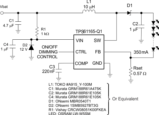
The default white LED current is set with the external sensor resistor Rset, and the feedback voltage is regulated to 200 mV, as shown in the Typical Application section. During the operation, the LED current can be controlled using the 1-wire digital interface (EasyScale™ protocol) through the CTRL pin. Alternatively, a pulse width modulation (PWM) signal can be applied to the CTRL pin through which the duty cycle determines the feedback reference voltage. In either digital or PWM mode, the TPS61165-Q1 device does not burst the LED current; therefore, the device does not generate audible noises on the output capacitor. For maximum protection, the TPS61165-Q1 device features integrated open LED protection that disables it to prevent the output from exceeding its absolute maximum voltage ratings during open LED conditions.
The TPS61165-Q1 device is available in a SOT-23 package.
Device Information(1)
| PART NUMBER | PACKAGE | BODY SIZE (NOM) |
|---|---|---|
| TPS61165-Q1 | SOT-23 (6) | 1.60 mm × 2.90 mm |
Typical Application Schematic
