SLVSBM5B December 2012 – August 2015 TPS61176
PRODUCTION DATA.
- 1 Features
- 2 Applications
- 3 Description
- 4 Revision History
- 5 Pin Configuration and Functions
- 6 Specifications
- 7 Detailed Description
- 8 Application and Implementation
- 9 Power Supply Recommendations
- 10Layout
- 11Device and Documentation Support
- 12Mechanical, Packaging, and Orderable Information
Package Options
Mechanical Data (Package|Pins)
- RTE|16
Thermal pad, mechanical data (Package|Pins)
- RTE|16
Orderable Information
10 Layout
10.1 Layout Guidelines
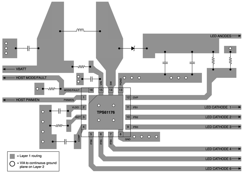
As for all switching power supplies, especially those providing high current and using high switching frequencies, layout is an important design step. If layout is not carefully done, the regulator could show instability as well as EMI problems. Therefore, use wide and short traces for high current paths. The input capacitor, C1 in Figure 9, needs not only to be close to the VIN pin, but also to the GND pin in order to reduce the input ripple seen by the device. It should also be placed close to the inductor. C3 is the filter and noise decoupling capacitor for the internal linear regulator powering the internal digital circuits. It should be placed as close as possible between the VLDO and GND pins to prevent any noise insertion to the digital circuits. The SW pin carries high current with fast rising and falling edges. Therefore, the connection between the SW pin to the inductor and Schottky diode should be kept as short and wide as possible. The trace between the Schottky diode and the output capacitor C2 should also be as short and wide as possible. It is also beneficial to have the ground of the output capacitor C2 close to the PGND pin because there is a large ground return current flowing between them. When laying out signal grounds, it is recommended to use short traces separated from power ground traces, and connect them together at a single point — for example, on the thermal pad. The thermal pad needs to be soldered onto the PCB and connected to the GND pin of the device. An additional thermal via can significantly improve power dissipation of the device.
10.2 Layout Example
 Figure 22. TPS61176 Layout